


Paper Sharing
【Member Papers】Progress in β-Ga₂O₃ Vertical Power Devices Achieved by the Nano Fabrication Platform of Suzhou Institute of Nano-Tech and Nano-Bionics
日期:2025-09-11阅读:864
As an ultra-wide bandgap (UWBG) semiconductor, gallium oxide (β-Ga₂O₃) is rapidly emerging as a disruptive force in post-Moore power electronics, owing to its outstanding ultra-high breakdown field strength of 8 MV/cm and unique advantage of large-size melt growth. Vertical power electronic devices, by optimizing the design of vertical blocking layers, can simultaneously achieve 10 kV-class high breakdown voltage and kA-class ultra-large current capability within a single chip area. This perfectly meets the urgent demands for ultra-high power density, high efficiency, and miniaturization in applications such as smart grids, new energy vehicles, industrial motor drives, data center power supplies, and renewable energy (photovoltaic and wind) converters.
Recently, the Nano Fabrication Platform of the Suzhou Institute of Nano-Tech and Nano-Bionics (SINANO), Chinese Academy of Sciences, has made two important breakthroughs in the field of β-Ga₂O₃ power devices: (1) for the first time, fabrication processes based on the platform were developed to prepare multi-fin-channel ohmic-contact anode β-Ga₂O₃ diodes (MFCDs), achieving kilovolt-class breakdown voltage with ultra-low leakage current; and (2) a high-performance enhancement-mode vertical β-Ga₂O₃ multi-fin transistor was realized, setting a record-low specific on-resistance of 4.3 mΩ·cm². These achievements provide brand-new solutions for high-temperature and high-voltage application scenarios.
Multi-Fin Channel Diode: Breaking the Limitations of Conventional Vertical Structures
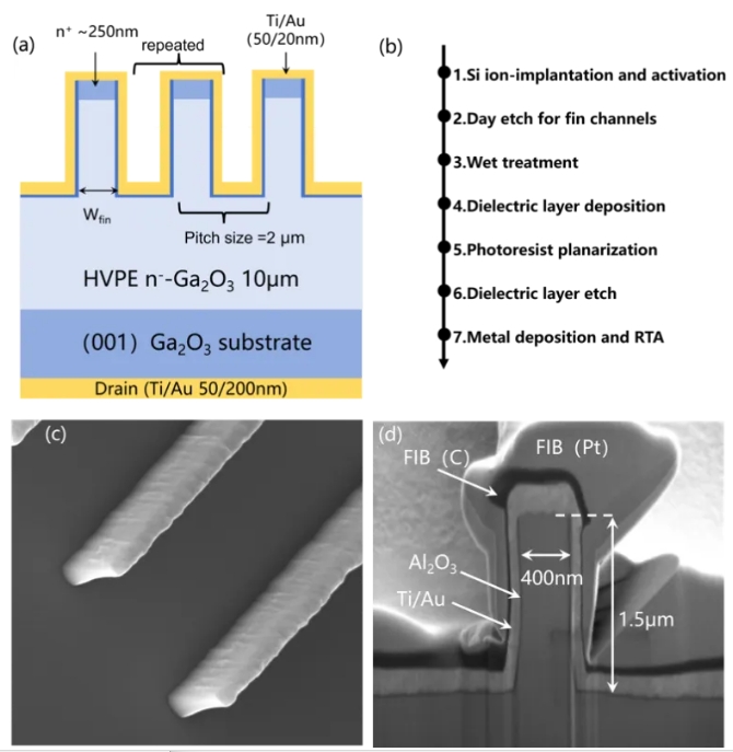
Fig. 1. (a) Schematic of the multi-fin channel β-Ga₂O₃ diode, (b) key fabrication steps of the device, (c) scanning electron microscope (SEM) image after fin dry etching, and (d) SEM cross-sectional image of a diode with a 400 nm fin width. The device adopts an innovative ohmic-contact anode design to replace the conventional Schottky structure. Combined with the sidewall self-depletion effect induced by the submicron fin channel, it successfully addresses the issue of leakage current runaway in wide-bandgap semiconductor devices under high electric fields. Without any field plate or passivation assistance, the narrow-fin (0.1 μm) device exhibits a breakdown voltage of 1148 V, with reverse leakage current stably maintained at a commercial level of 1 μA/cm², and no performance degradation observed even at an elevated temperature of 150 °C. The introduction of the ohmic contact reduces the specific on-resistance to 7 mΩ·cm², representing a 35% reduction compared to similar trench Schottky diodes. This breakthrough provides a novel solution for high-voltage applications such as photovoltaic inverters and fast-charging stations for electric vehicles.
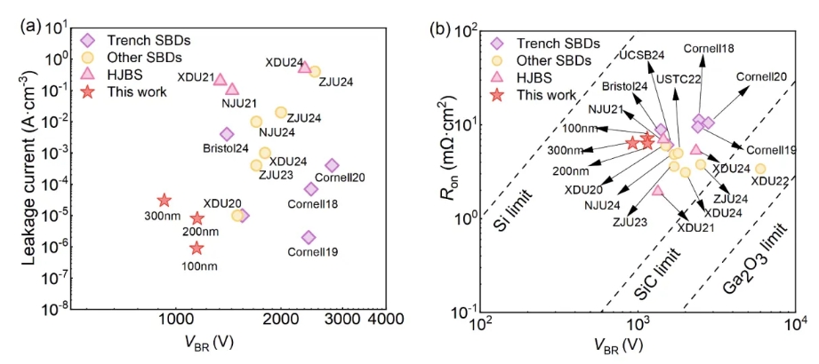
Fig. 2. (a) comparison of the leakage current and breakdown voltage reference performance of the vertical diode, (b) comparison of the on-resistance and breakdown voltage reference performance of the β-Ga2O3 vertical diode and the trench SBD in this work, as well as the comparison of the results reported in the literature.
The results were presented at IEEE 37th International, the top international conference in the field of power electronic devices, under the title "Kilovolt-Class β
-Ga2O3 Multi-Fin-Channel Diodes with Ohmic Contact Anode" Symposium on Power Semiconductor Devices and ICs 2025. The first authors are Gao Fu Guo and Zhang Xiaodong from Suzhou Institute of Nano-Tech and Nano-Bionics, Chinese Academy of Sciences. The corresponding authors are Researcher Baoshun Zhang and Professor Xianqi Dai from Henan Normal University.
Enhancement-Mode Vertical Transistor — Cracking the “Normally-On” Challenge
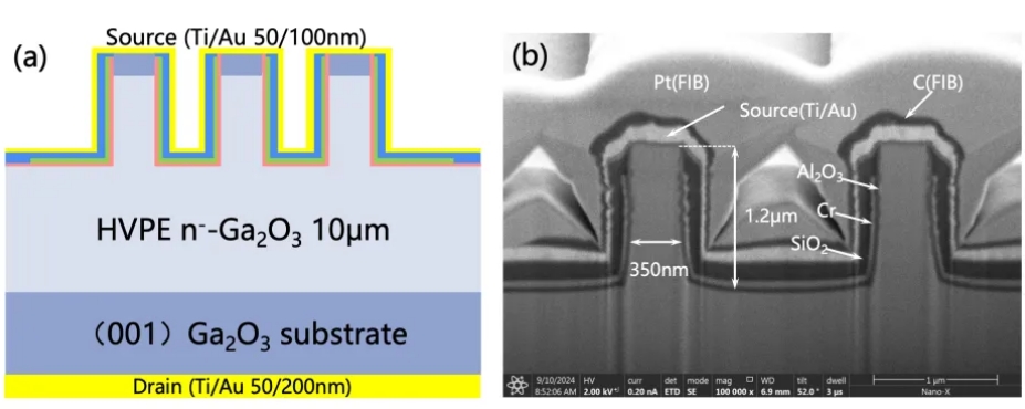
Fig. 3. (a) Schematic of the multi-fin-channel β-Ga₂O₃ FinFET; (b) SEM cross-sectional image of a diode with a fin width of 300 nm.
Addressing the core bottleneck of the lack of p-type doping in gallium oxide materials, the research team has simultaneously developed a world-leading enhancement-mode vertical multi-fin transistor. By employing a dual-gate fin-channel geometric confinement technique, reliable normally-off operation is achieved without relying on p-type layers, with a threshold voltage of 0.87 V and an on/off ratio exceeding 7×10⁶. Innovatively, electron-beam lithography combined with non-metallic mask etching enables precise control of 350 nm fin widths, while dual self-aligned planarization technology is used to accurately construct the source and drain contact regions. The final device delivers an ultra-high current density of 760 A/cm² at 10 V operating voltage, with an ultra-low specific on-resistance of only 4.3 mΩ·cm², while maintaining a breakdown voltage of 975 V and an excellent power figure of merit (PFOM) of 0.22 GW/cm². This breakthrough lays a key technological foundation for the domestic development of power supply chips for data centers and industrial motor drives.
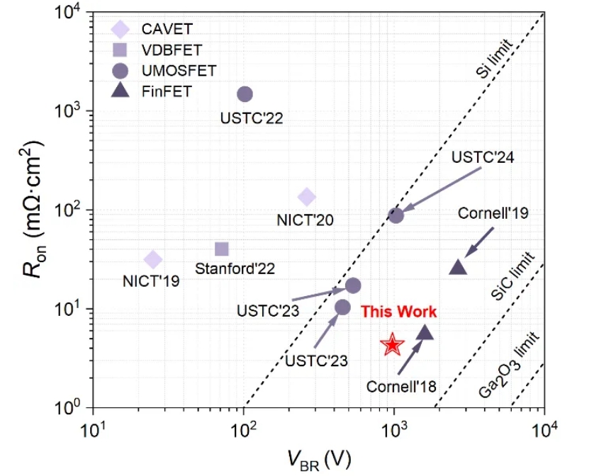
Fig. 4. Performance comparison of Vbr and R(on,sp) for the latest vertical β-Ga₂O₃ MOSFET devices.
This achievement was published under the title “975 V/4.3 mΩ·cm² Enhancement-mode (001) β-Ga₂O₃ Vertical Multi-fin Power Transistors” at the 9th IEEE Electron Devices Technology and Manufacturing Conference (EDTM 2025), an international conference in the semiconductor field. The first author is Gao-Fu Guo from the Suzhou Institute of Nano-Tech and Nano-Bionics, Chinese Academy of Sciences, and the corresponding authors are Researcher Baoshun Zhang and Professor Xianqi Dai from Henan Normal University. This work was supported by the National Key R&D Program of China, the National Natural Science Foundation of China, the Nanchang Key Laboratory Construction Project, and the Jiangxi Province Double Thousand Plan. It also received strong support from the Nano-Fabrication Platform, the Testing Platform, the Nano Device Research Division, and the Nano-X Vacuum Interconnected Experiment Station at the Suzhou Institute of Nano-Tech and Nano-Bionics, Chinese Academy of Sciences.
