


Paper Sharing
【Member Papers】Energy-band engineering and deep-ultraviolet photodetection of Ga₂O₃ alloys: a concise review
日期:2025-09-11阅读:811
Researchers from the Inner Mongolia University and Nanjing University of Posts and Telecommunications have published a dissertation titled "Energy-band engineering and deep-ultraviolet photodetection of Ga2O3 alloys: a concise review" in Nanotechnology.
Project Support
This work is supported by the Young Scientists Fund of the National Natural Science Foundation of China (Grant No. 62204125), the Inner Mongolia University Experimental Technology Research Project in 2025 (Self-Made and Modified Equipment Project) (Grant No. SYJS2025004), the Steed Plan of Inner Mongolia University for Introducing High-Level Talents (Grant Nos. 10000-23112101/285 and 10000-23112101/277), the Program for Innovative Research Team in Universities of Inner Mongolia Autonomous Region (GrantNo.NMGIRT2503), the Joint Funds of the Natural Science Foundation of China (Grant No. U23A20349), the Key Technology Project of Suzhou City (Grant No. SYG2024003),and the Jiangsu Provincial Team of Innovation and Entrepreneurship(GrantNo.JSSCTD202351).
Abstract
Gallium oxide (Ga2O3)-based solar-blind ultraviolet photodetectors gained much attention for their promising prospects in new-generation solid-state optoelectronics and electronics. Catering for the demands of broadband photodetection, tunable energy-band, adjusted carrier concentration and effective carrier transition, alloying engineering through doping is gradually launched as one of the research emphases. This review is proposed to understand the photodetection performances in view of energy-band engineering. Especially for the representative (InxGa1−x)2O3 and (AlyGa1−y)2O3 alloys, the conduction band edges upshift as the empty Al 3 s and In 5 s states are introduced with higher energy, hybridize with Ga 4 s state. This leads to a result that low effective electron mass and high electron mobility could be achieved, contributing to high quality tunable performances of solar-blind UV photodetection. Thus, in this concise review article, the alloyed Ga2O3 for photodetection would be reviewed and discussed based on the current developments, from the viewpoint of energy-band theory.
Outlook and perspectives
In summary, this concise review has highlighted significant progress and ongoing efforts in energy-band engineering and tunable deep UV (DUV) photodetection. Alloying—particularly with similarly structured group III elements like In and Al—as well as doping with other elements (e.g., N, Ir, Ti, Zn) or managing intrinsic defects, provides powerful routes to modulate the bandgap, adjust carrier concentration, and modify carrier transport dynamics. These capabilities are crucial for optimizing photodetector performance, including wavelength selectivity, photoresponsivity, and response speed, catering to diverse applications from flame sensing to secure communication.
Despite the promising advancements, several key challenges and exciting opportunities remain:
1.P-type doping: Achieving stable, reliable, and efficient p-type conductivity in wide-bandgap Ga₂O₃ and its alloys remains a critical bottleneck. While some progress has been made (e.g., N-doping, Ir-alloying), overcoming issues such as self-compensation by native defects and low acceptor solubility is paramount for realizing high-performance bipolar devices like p–n homojunctions. Future work exploring novel acceptor dopants, co-doping strategies, or non-equilibrium growth techniques is essential.
2.Defect control and understanding: While doping and alloying enable bandgap tuning, they inevitably introduce defects (point defects, complexes, dislocations, grain boundaries). These defects can act as trapping or recombination centers, detrimentally affecting carrier lifetime, mobility, and device stability. A deeper understanding of defect formation mechanisms, their energy levels within the bandgap, and their precise impact on optoelectronic properties—assisted by advanced characterization and synergistic computational modeling—is crucial. Developing effective defect passivation or mitigation strategies during material growth and device processing is a key area for improvement.
3.Alloy homogeneity and phase stability: Achieving uniform composition and maintaining phase stability, especially at higher alloying concentrations needed for significant bandgap shifts, can be challenging due to lattice mismatch and differing thermodynamic properties. Further optimization of growth techniques is needed to minimize phase segregation and structural imperfections that degrade material quality and device performance.
4.Device integration and reliability: Translating improved material properties into robust, reliable, and manufacturable devices requires overcoming challenges in contact formation, surface passivation, device packaging, and long-term stability under operational stress.
Looking forward, the field of Ga₂O₃ alloy-based DUV photodetectors holds immense potential. Continued interdisciplinary efforts combining materials science, physics, chemistry, and device engineering will be vital. Addressing the aforementioned challenges will pave the way for next-generation DUV optoelectronic devices with unprecedented performance and functionalities, impacting fields ranging from environmental monitoring and industrial process control to defense and space exploration.
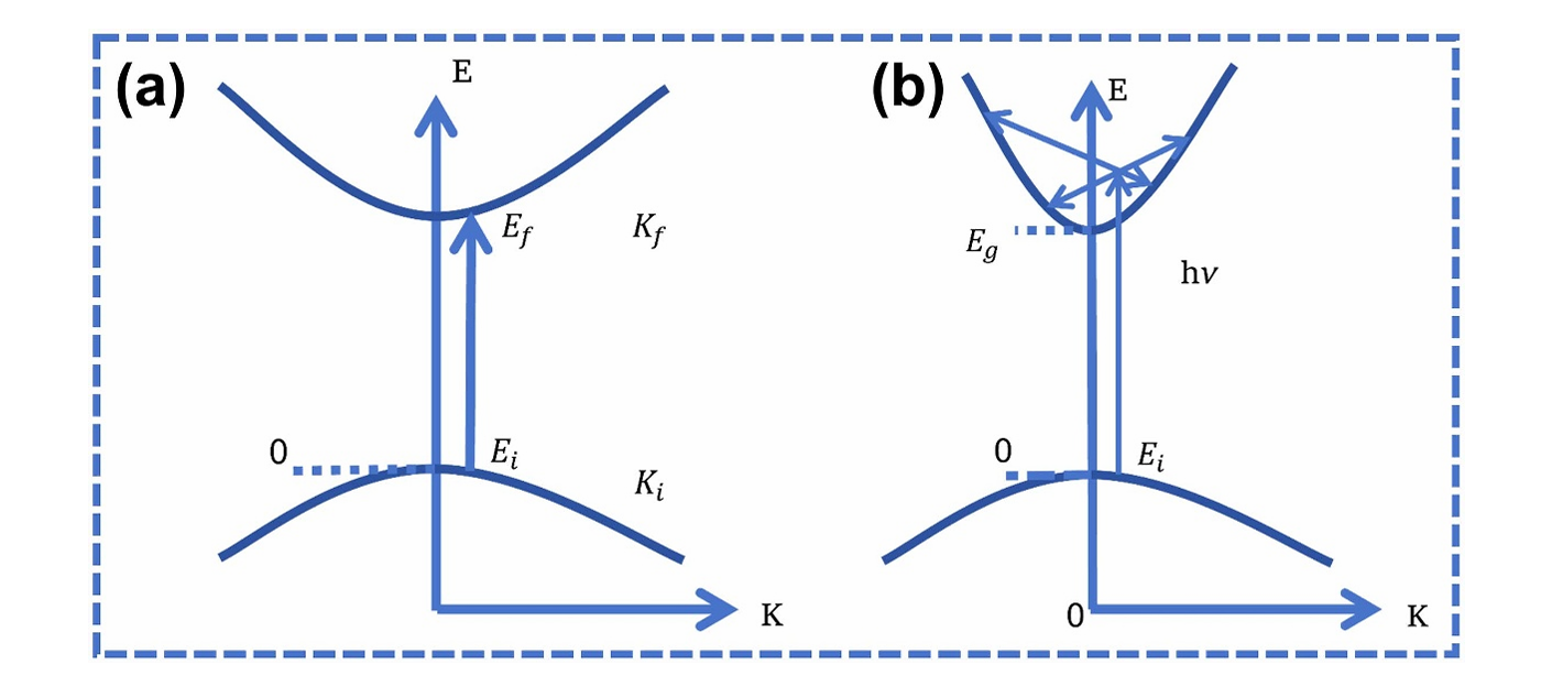
Figure 1. Schematic diagrams of (a) allowed direct transition and (b) indirect transition for direct energy-band semiconductor.
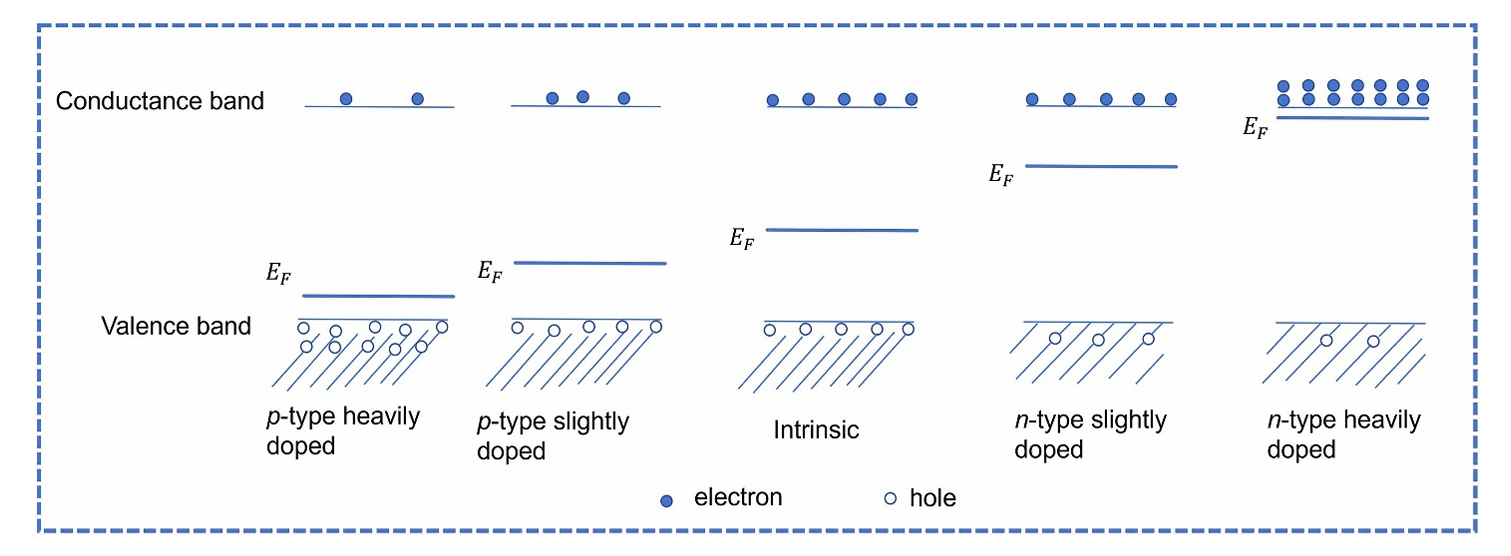
Figure 2. Energy-band diagrams for understanding the band-to-band carrier transports: effects of doping concentration on the carrier concentration and location of EF
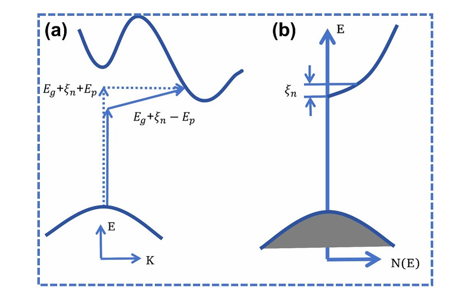
Figure 3. Schematic diagrams of (a) energy-quantity of motion and (b) energy-density of states for direct energy-band degenerate n-type semiconductor.
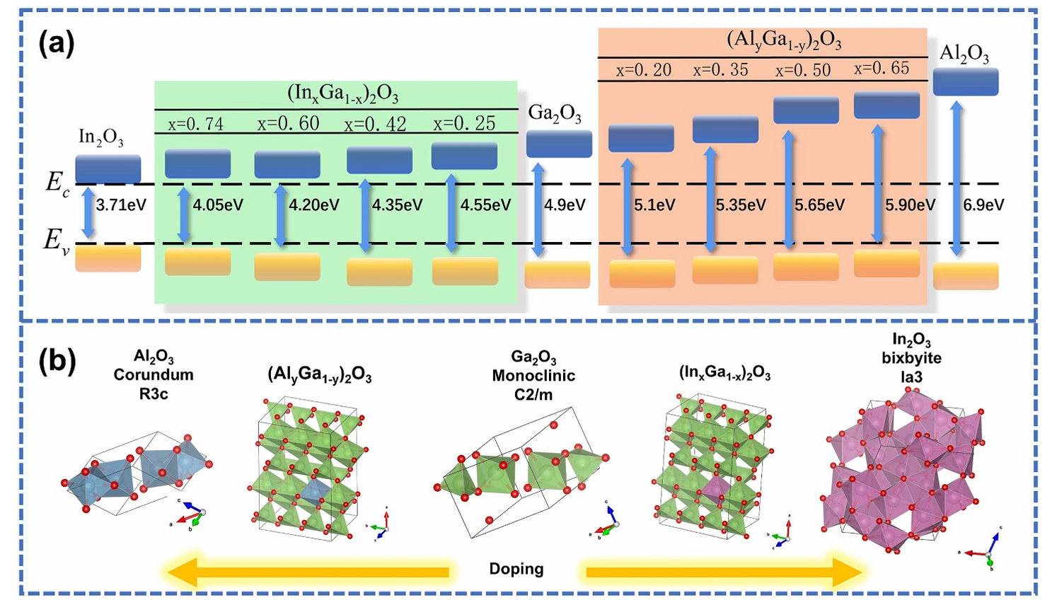
Figure 4. (a) The diagram of the energy band and (b) the crystal structures for (InxGa1−x)2O3 and (AlyGa1−y)2O3.
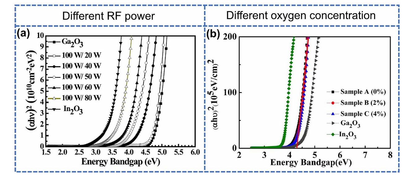
Figure 5. (a) Absorbance coefficient spectra measured from the as-deposited (InxGa1−x)2O3 thin films, indicating optical bandgap from 3.4 to 4.9 eV, as the radio-frequency sputtering power for the In2O3 target was decreased. (b) Tauc’s plots and linear fitting of the absorbance spectra of Ga2O3, In2O3 and (InxGa1−x) 2O3 samples with different oxygen flow concentrations.
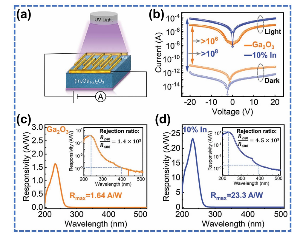
Figure 6. Schematic diagrams of the device structure and performance comparison for Ga2O3 and (InxGa1−x)2O3 photodetectors, where the In concentration was 10% in their report: (a) the photodetector structure, (b) I–V curves of Ga2O3 and (In0.1Ga0.9)2O3 photodetectors in the dark and under 254 nm light. Response spectra of (c) Ga2O3 and (d) (In0.1Ga0.9)2O3 photodetectors, in which the (In0.1Ga0.9)2O3 had higher responsivity.
DOI:
doi.org/10.1088/1361-6528/ae0043
