Paper Sharing
【International Papers】Enhanced Device Characteristics of Hybrid-Channel (Poly-Si/IGO) Structures with Ga₂O₃ and Al₂O₃ Interlayers by Suppressing Oxidation-Induced Variability for Ultra-High-Density 3D NAND Flash Memory Applications
日期:2025-09-12阅读:657
Researchers from the Hanyang University have published a dissertation titled "Enhanced Device Characteristics of Hybrid-Channel (Poly-Si/IGO) Structures with Ga2O3 and Al2O3 Interlayers by Suppressing Oxidation-Induced Variability for Ultra-High-Density 3D NAND Flash Memory Applications" in Advanced Functional Materials.
Background
3D NAND flash memory has become a key non-volatile storage technology due to its ability to dramatically increase density through stacking. However, conventional poly-Si channels suffer from grain boundary defects, leading to severe threshold voltage variation and current degradation, which become critical in ultra-high stacking (>300 layers). Although oxide semiconductors offer high mobility and uniformity, their wide bandgap limits GIDL-based erase operations. Hybrid poly-Si/IGO channels have been introduced to combine erase capability with high mobility, but high-temperature annealing (~800 °C) induces interfacial oxidation, degrading device stability and performance.
To address this, the present work introduces ultrathin Ga₂O₃ or Al₂O₃ interlayers between poly-Si and IGO channels to suppress interfacial oxidation and enhance device characteristics, validated through TCAD simulations and experimental measurements.
Abstract
Hybrid-channel (HC) structures integrating polycrystalline silicon (poly-Si) and oxide semiconductors offer a promising path toward high-mobility, thermally stable architectures for next-generation 3D NAND flash memory. However, high-temperature annealing required for oxide crystallization often induces interfacial oxidation, leading to device variability and degraded performance. To address this challenge, this study proposes a novel HC structure incorporating an ultrathin interlayer of Ga2O3 or Al2O3 between the poly-Si and In-Ga-O (IGO) channels. This interfacial layer effectively suppresses poly-Si loss and the formation of non-uniform interfacial oxide, reducing poly-Si degradation from 5 to 1.7 nm and interfacial oxide growth from 7.4 to 2.5 nm. As a result, threshold voltage variation improves significantly, from ±0.45 to ±0.24 V and ±0.40 V for Ga2O3 and Al2O3, respectively, while average cell current density increases from 1.87 to over 2.0 µA µm−1. Memory windows expand accordingly, and both interlayers enable a field-effect mobility exceeding 100 cm2 V·s−1. These findings demonstrate the importance of interfacial engineering in HC devices and establish a viable route for integrating thermally stable oxide semiconductors into ultra-high-density 3D memory applications.
Conclusion
In this paper, we investigated the device characteristics of the proposed HC structure, which incorporates an interlayer between the poly-Si and IGO channels. The proposed HC structure was fabricated and measured to validate its device performance.
The measurement results showed that the Vth variation decreased from ±0.45 V to ±0.24 V and ±0.40 V for Ga₂O₃ and Al₂O₃, respectively, while the average Icell density increased from 1.87 to 2.04 μA/μm and 2.01 μA/μm. Additionally, the proposed HC structure achieved memory windows of 5.04 and 3.34 V for Ga₂O₃ and Al₂O₃, respectively, compared to 3.59 V in the conventional HC structure without an interlayer. Both Ga₂O₃ and Al₂O₃ achieved a μFE exceeding 100 cm²/V·s. These improvements resulted from the effective reduction of poly-Si loss from 5 to 1.7 nm and the suppression of interfacial oxide growth from 7.4 to 2.5 nm, even under high-temperature processing conditions. Furthermore, we verified the effectiveness of Ga₂O₃ and Al₂O₃ interlayers in enhancing the performance of the proposed HC structure.
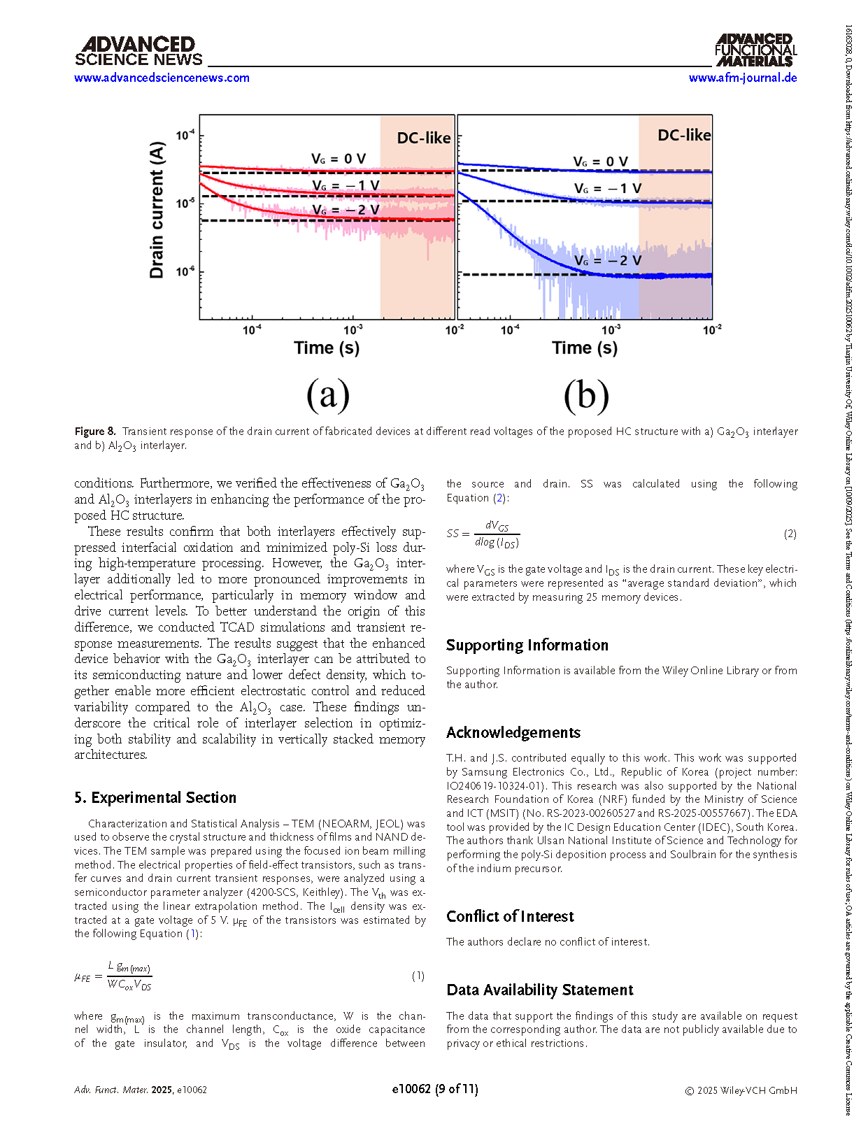
These results confirm that both interlayers effectively suppressed interfacial oxidation and minimized poly-Si loss during high-temperature processing. However, the Ga₂O₃ interlayer additionally led to more pronounced improvements in electrical performance, particularly in memory window and drive current levels. To better understand the origin of this difference, we conducted TCAD simulations and transient response measurements. The results suggest that the enhanced device behavior with the Ga₂O₃ interlayer can be attributed to its semiconducting nature and lower defect density, which together enable more efficient electrostatic control and reduced variability compared to the Al₂O₃ case. These findings underscore the critical role of interlayer selection in optimizing both stability and scalability in vertically stacked memory architectures.
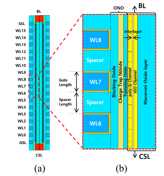
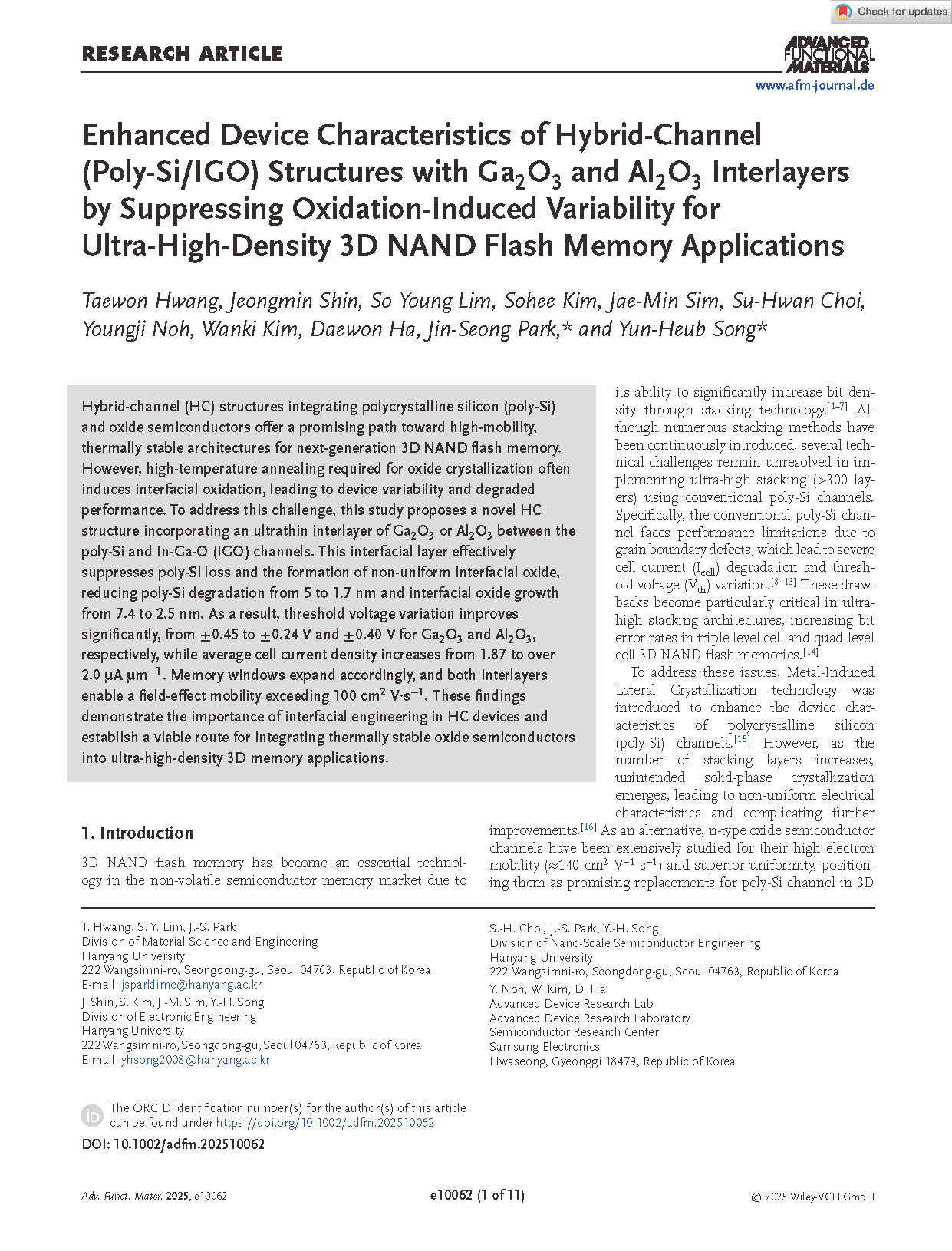
Figure 1. a) 3D NAND flash memory string with the proposed HC structure and b) detailed HC structure with 3 WLs based on the ONO stack.
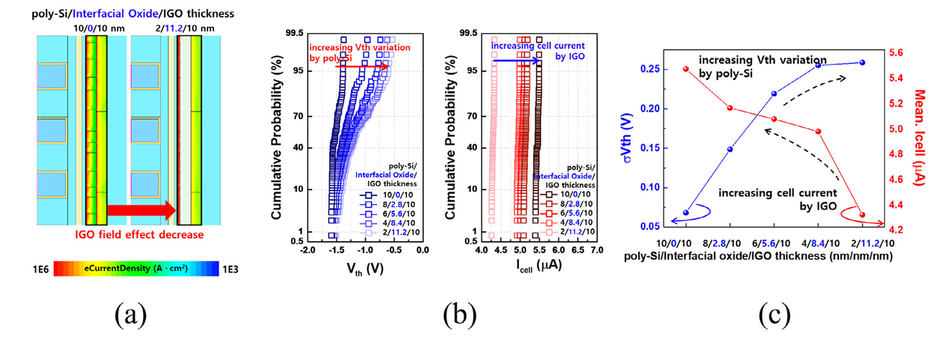
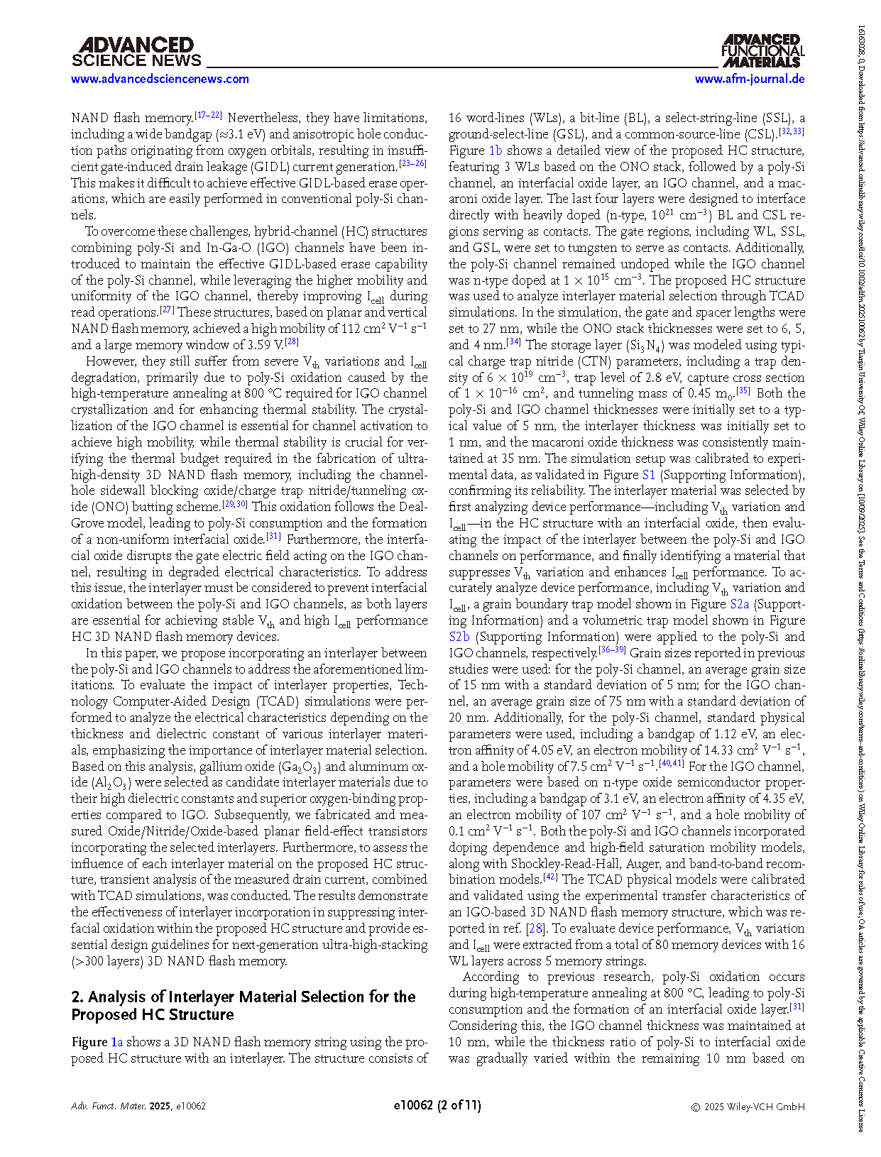
Figure 2. a) Simulation results of electron current density in the HC structure with interfacial oxide, b) cumulative probability distributions of Vth and Icell, and c) standard deviation of Vth and mean value of Icell at various poly-Si and interfacial oxide thicknesses (with a fixed IGO thickness of 10 nm).
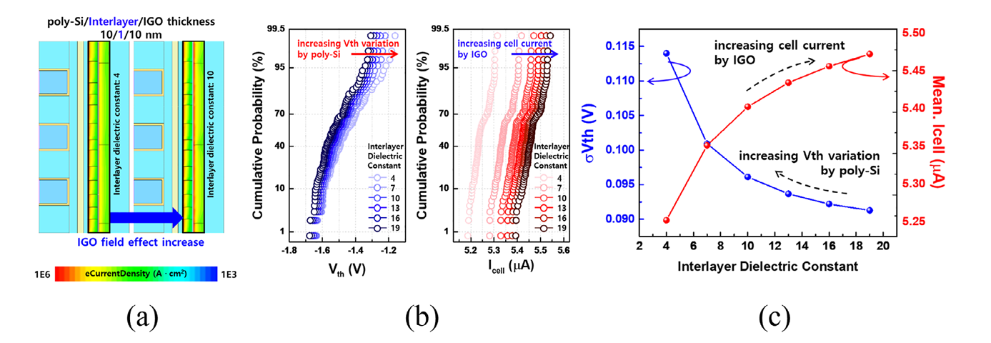
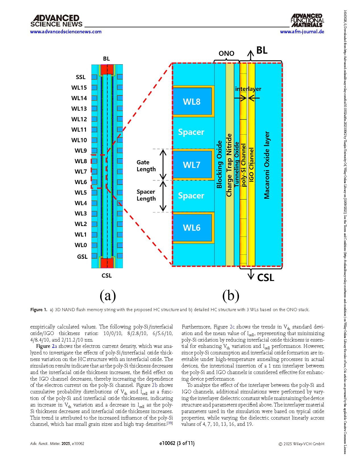
Figure 3. a) Simulation results of electron current density in the proposed HC structure, b) cumulative probability distribution of Vth and Icell at different interlayer dielectric constants, and c) standard deviation of Vth and mean value of Icell as functions of the interlayer dielectric constant.
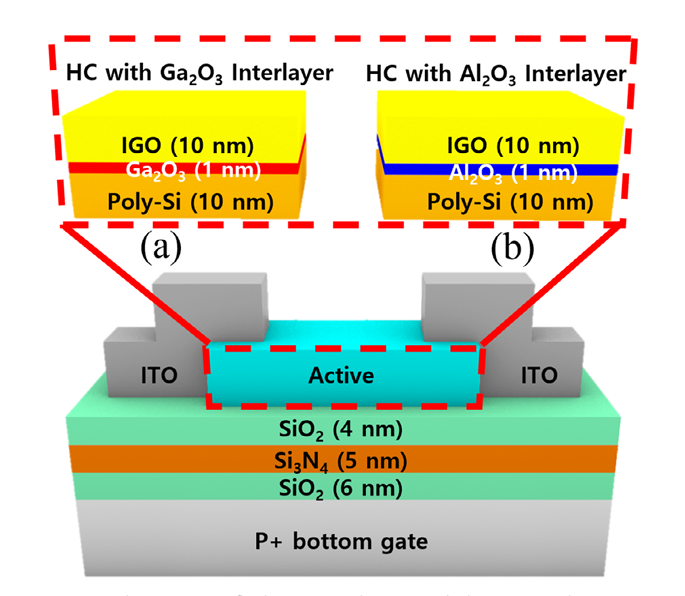
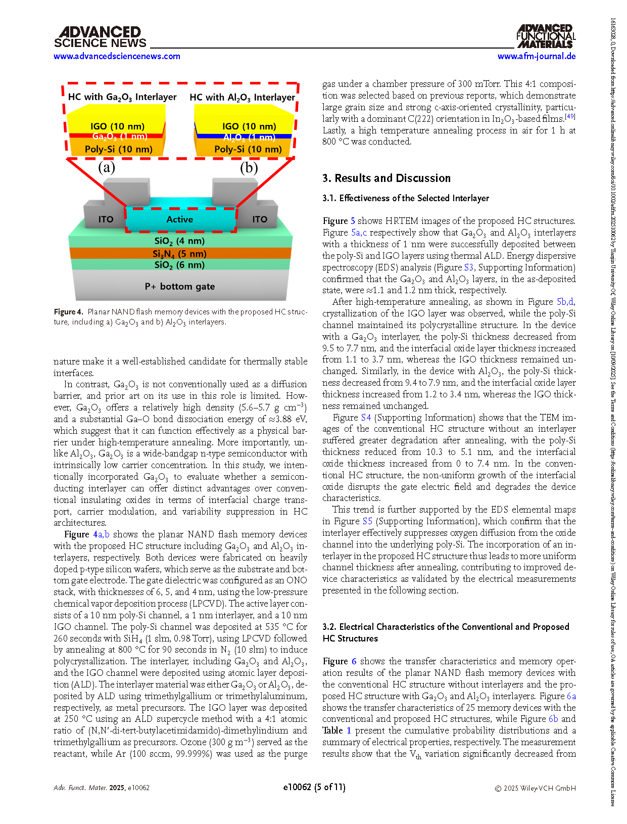
Figure 4. Planar NAND flash memory devices with the proposed HC structure, including a) Ga2O3 and b) Al2O3 interlayers.
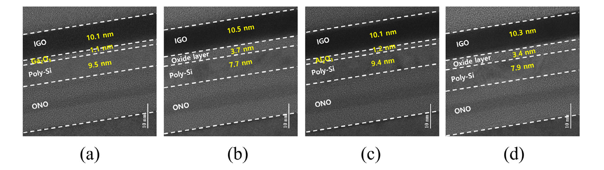
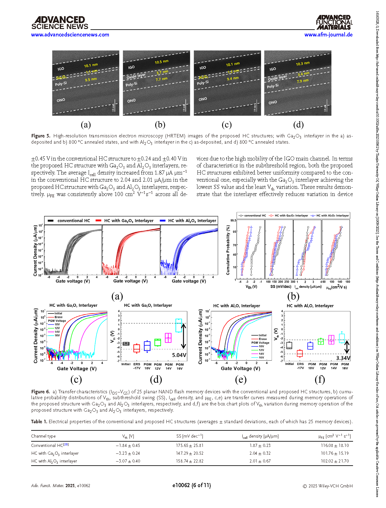
Figure 5. High-resolution transmission electron microscopy (HRTEM) images of the proposed HC structures; with Ga2O3 interlayer in the a) as deposited and b) 800 °C annealed states, and with Al2O3 interlayer in the c) as-deposited, and d) 800 °C annealed states.

Figure 6. a) Transfer characteristics (IDS–VGS) of 25 planar NAND flash memory devices with the conventional and proposed HC structures, b) cumu lative probability distributions of Vth, subthreshold swing (SS), Icell density, and μFE, c,e) are transfer curves measured during memory operations of the proposed structure with Ga2O3 and Al2O3 interlayers, respectively, and d,f) are the box chart plots of Vth variation during memory operation of the proposed structure with Ga2O3 and Al2O3 interlayers, respectively.
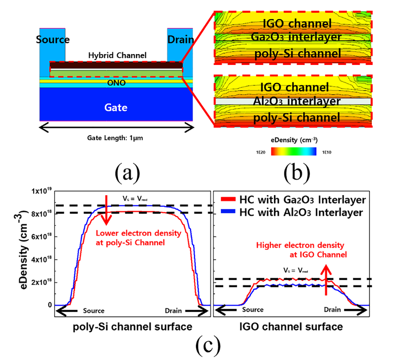
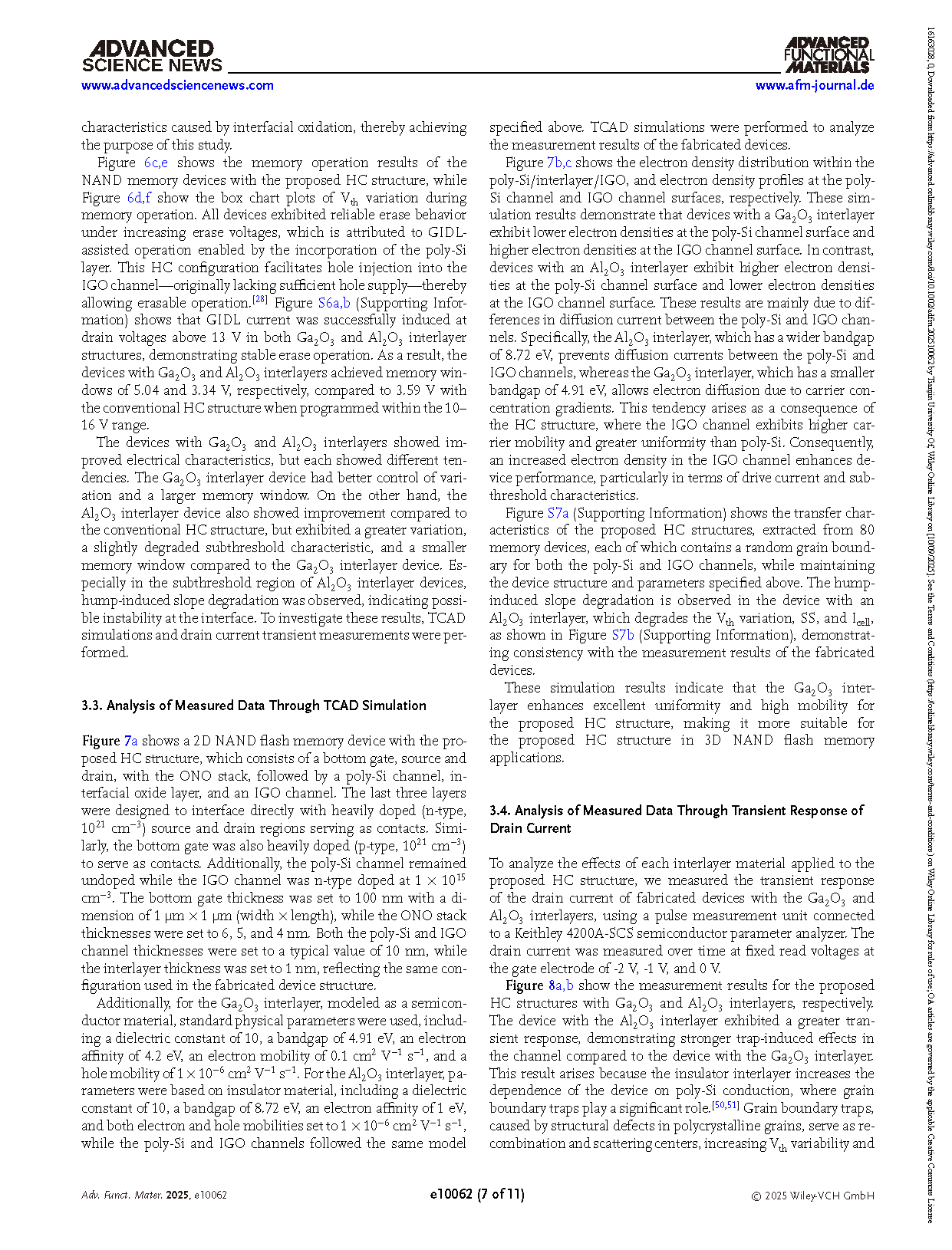
Figure 7. a) 2D NAND flash memory device with the proposed HC structure, b) electron density distributions with different interlayers (Ga2O3 and Al2O3), and c) electron density profiles at the poly-Si and IGO channel surfaces, depending on different interlayers.
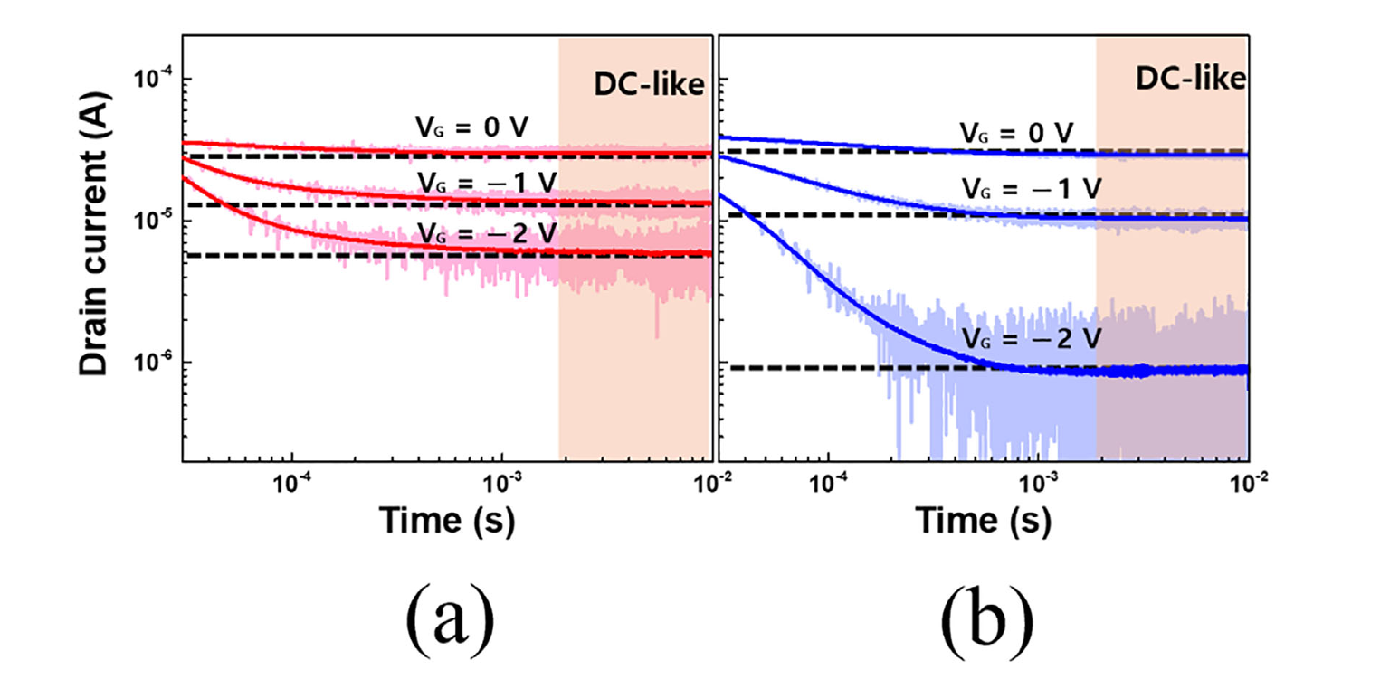
Figure 8. Transient response of the drain current of fabricated devices at different read voltages of the proposed HC structure with a) Ga2O3 interlayer and b) Al2O3 interlayer.
DOI:
doi.org/10.1002/adfm.202510062