Paper Sharing
【Domestic Papers】Simulation Study on Electrical Characteristics of NiO/β-Ga₂O₃ Heterojunction Enhancement Mode HJ-FinFET
日期:2025-09-18阅读:639
Researchers from the North University of China have published a dissertation titled "Simulation Study on Electrical Characteristics of NiO/β-Ga2O3 Heterojunction Enhancement Mode HJ-FinFET" in Crystals.
Project Support
This research was supported by the Key Research and Development Program of Shanxi Province (Grant NO. 202302030201001) and Supported by the science and technology major Program of Shanxi Province (Grant NO. 202301030201003).
Background
Due to the lack of effective P-type doping and low electron mobility, the voltage resistance of gallium oxide power devices is still far below the theoretical value and current research mainly focuses on exploring methods to alleviate the phenomenon of electric field concentration through small-sized devices, but there is relatively little research on large-sized high-power devices and their thermal stability. In addition, the low thermal conductivity of gallium oxide materials, coupled with complex intrinsic defect energy-level distribution, process defects, interface states, and oxide layer traps, lead to reliability issues such as electrical characteristic drift and accelerated performance degradation in gallium oxide devices.
In this paper, a novel Ga2O3 FinFET with NiO/n-Ga2O3 heterojunction (named Heterojunction FinFET: HJ-FinFET) for E-mode-type operation has been proposed. The p-NiO layer dramatically improves Vbr; meanwhile, p-NiO/n-Ga2O3 forms an HJ and hetero-reduces the reverse conducting loss. It is expected that the proposed structure can cause the threshold voltage to shift to the right and realize the design of E-mode devices, and this device can be fabricated through ALD, MOCVD and lithography techniques.
Abstract
In this paper, a novel enhancement-mode β-Ga2O3-based FinFET structure with a gate formed by the NiO/β-Ga2O3 heterojunction named HJ-FinFET has been proposed, and the excellent performance of the device has also been demonstrated. The primary operational mechanism of this structure involves integrating p-type NiO on both sides of the fin-shaped channel, which forms p-n junctions with β-Ga2O3. The depletion regions thus generated are utilized to establish electron channels, enabling enhancement-mode operation. The reverse p-NiO/n-Ga2O3 heterojunction diode is integrated to reduce the reverse free-wheeling loss. Compared with the conventional devices, the threshold voltage of the HJ-FinFET is greatly improved, and normally off operation is realized, showing a positive threshold voltage of 2.14 V. Meanwhile, the simulated breakdown voltage of the HJ-FinFET reaches 2.65 kV with specific on-resistance (Ron,sp) of 2.48 mΩ·cm2 and the power figure of merit (PFOM = BV2/Ron,sp) reaches 2840 MW/cm2, respectively. In addition, the influence of the doping concentration of the heterojunction layer constituting the gate, the doping concentration of the drift layer, and the channel width on the electrical characteristics of the devices were focused on. This structure provides a feasible idea for high-performance β-Ga2O3-based FinFET.
Conclusions
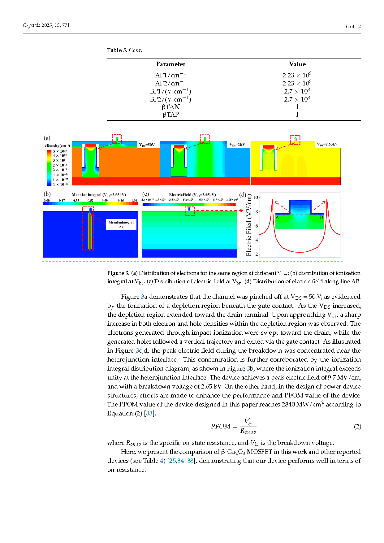
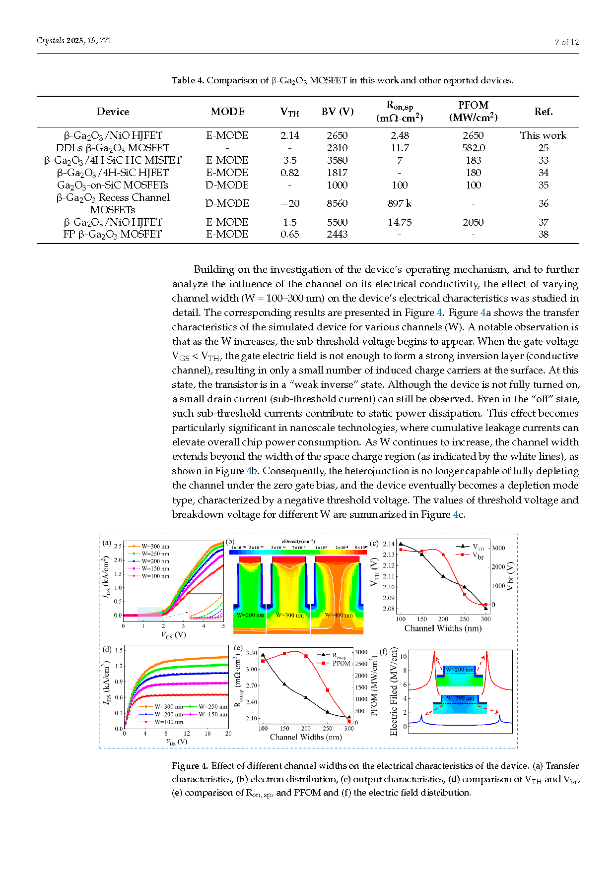
In this work, a novel E-mode NiO/β-Ga2O3 HJ-FinFET has been proposed and investigated to achieve high-performance E-mode β-Ga2O3-based FinFETs. The influence of the doping concentration of the heterojunction layer constituting the gate, the doping concentration of the drift layer, and the channel width on the electrical characteristics of the devices were focused on. The simulation results shown that the width of the channel and the doping concentration of the β-Ga2O3 layer are the dominant factors affecting the device characteristics. By optimizing the relevant parameters, the device can operate stably in E-mode and a higher breakdown voltage was obtained. Ultimately, the device achieved a turn-on voltage of 2.14 V, a breakdown voltage of 2.65 kV, a low specific on-resistance (Ron,sp) of 2.48 mΩ·cm2, and a high PFOM of 2840 MW/cm2. In summary, the novel architecture proposed in this study effectively overcomes the common performance limitations of traditional lateral β-Ga2O3 MOSFETs. This advancement enables the realization of E-mode-type β-Ga2O3-based FinFET with low specific on-state resistance (Ron,sp) and high breakdown voltage, thus providing a new method for achieving high-performance power devices.
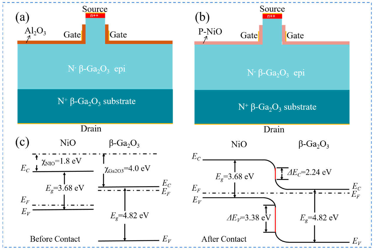
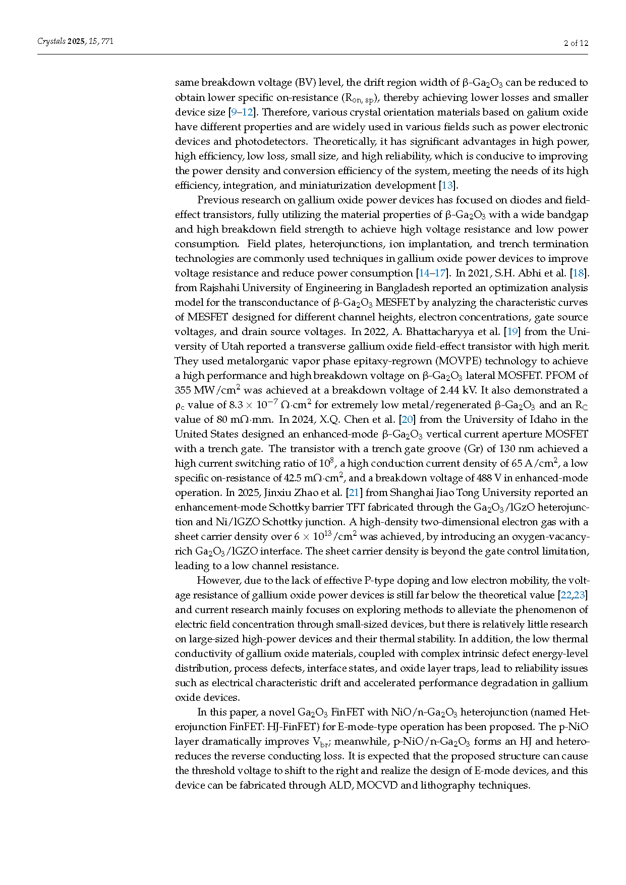
Figure 1. Illustration of Fin-FET: (a) conventional β-Ga2O3-based FinFET; (b) β-Ga2O3-based HJ-FinFET; (c) schematic energy band diagram of the NiO/Ga2O3.
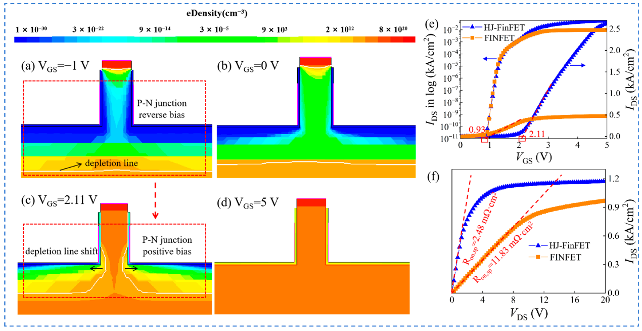
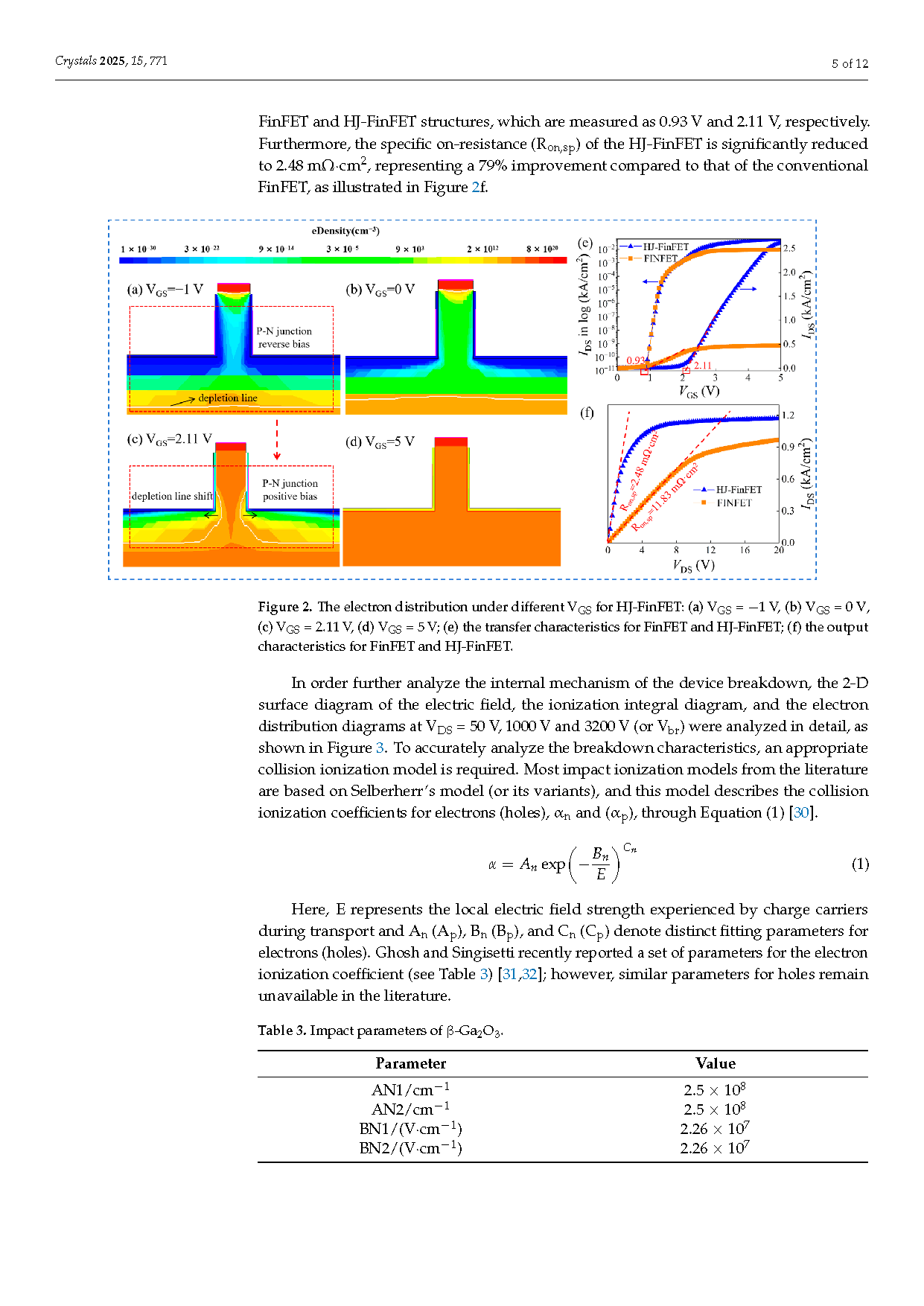
Figure 2. The electron distribution under different VGS for HJ-FinFET: (a) VGS = −1 V, (b) VGS = 0 V, (c) VGS = 2.11 V, (d) VGS = 5 V; (e) the transfer characteristics for FinFET and HJ-FinFET; (f) the output characteristics for FinFET and HJ-FinFET.
DOI:
doi.org/10.3390/cryst15090771