


Paper Sharing
【International Papers】Lateral Semiconductor–Free-Space Gate Transistors
日期:2025-10-15阅读:534
Abstract
We introduce a novel lateral transistor architecture, the semiconductor–free-space gate transistor (SFGT), in which the conventional solid dielectric is replaced by a semiconductor–free-space gate configuration with sub-100 nm fin channels and dual side gates. This work presents the first demonstration of free-space gating in wide and ultrawide bandgap semiconductors, achieving performance on par with oxide-gated transistors. SFGTs fabricated using β-Ga2O3 exhibit subthreshold slopes below 200 mV/dec, high drain current exceeding 250 mA/mm, hysteresis under 230 mV, ION/IOFF ratios above 106, and breakdown voltages over 500 V. The absence of a solid dielectric layer, combined with the open gate geometry, enables direct access to the gate region for external electric field modulation and threshold voltage tuning, while mitigating the detrimental effects of charges and trap states in conventional dielectrics. These results show the potential of SFGTs for future memory, sensing, and power applications.
Field effect transistors (FETs) modulate the flow of carriers in a channel through an externally applied voltage. They are fundamental components of modern technology, integral to devices such as microprocessors, memory modules, and sensors. In traditional metal-oxide-semiconductor (MOS) FETs, the applied voltage generates an electric field that penetrates the oxide dielectric and reaches the semiconductor, modulating the conductivity of the channel. Dielectric materials such as SiO2 and Al2O3 are commonly used as insulating layers to achieve this effect. The electric field that reaches and modulates the semiconductor channel is influenced by charges located within the dielectric material and at the dielectric–semiconductor interface, as well as by the intrinsic properties of the dielectric. This influence can be either beneficial or detrimental, depending on the degree of control over the involved charges. The undesired presence of oxide trap charges, interface trapped charges, and mobile ion charges within the dielectric can significantly degrade device performance. For example, the threshold voltage (VTH) of transistors subjected to extreme environments─such as high radiation or high temperatures─can be severely affected by such charges. Furthermore, at high temperature, trap states in the dielectric are known to contribute to various leakage mechanisms in transistors. Fowever, when properly controlled, these charges can be harnessed for VTH tuning, as well as for memory and sensing applications.
In recent years, the surge in demand for electronics in every aspect of our life has led to the development of novel device architectures and the integration of new materials into electronic devices. For instance, FETs based on 2D materials are currently under extensive investigation globally to meet the demands of several emerging applications. Likewise, other novel FET architectures such as optical gated FETs, van der Waals gap transistors, etc. have emerged to meet the demands of high-voltage, high-frequency and/or logic applications.
This letter presents the first demonstration of a free-space gated transistor in wide bandgap and ultra wide bandgap semiconductors. The device, referred to as the semiconductor–free-space gate transistor (SFGT), is a novel lateral transistor architecture with sub-100 nm fin width (WFIN) channel and dual side-gates, replacing the conventional solid dielectric with a semiconductor–free-space gate configuration, and for the first time achieves free-space gated performance on par with oxide-gated transistors. SFGTs fabricated using β-Ga2O3 exhibit subthreshold slopes (SS) below 200 mV/dec, high drain current (ID) exceeding 250 mA/mm, hysteresis (ΔVTH) less than 230 mV, an ION/IOFF ratio above 106, and a breakdown voltage (VBR) over 500 V. Moreover, the absence of a solid dielectric layer─combined with the open device geometry─provides direct access to the gate region, enabling external modulation of the electric field and threshold voltage (VTH) tuning through the deliberate introduction of charges or controlled modifications to the gate free space. This configuration also mitigates the detrimental effects associated with undesired charges and trap states in conventional dielectrics.
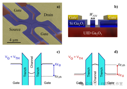
Figure 1. (a) Bird-view SEM image of the SFGT. (b) 3D schematic illustrating the cross-sectional view of the device channel. Energy band diagrams of the SFGT under (c) closed-channel (VG < VTH) and (d) open-channel (VG > VTH) conditions.

Figure 2. (a) Dual-sweep semilog transfer characteristics and (b) output characteristics of the β-Ga2O3 SFGT measured in air.
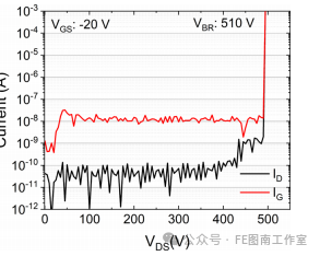
Figure 3. Breakdown characteristics of β-Ga2O3 SFGT for a device with WFIN of ∼65 nm.
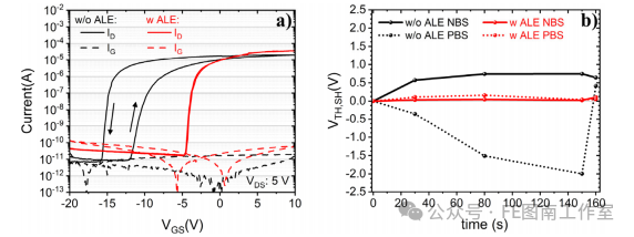
Figure 4. (a) Dual-sweep semilog transfer characteristics of a β-Ga2O3 SFGT with WFIN ∼ 90 nm. (b) VTH,SH under negative bias stress (NBS, −20 V) and positive bias stress (PBS, 20 V) for a device with WFIN of ∼65 nm. Both measurements were performed in air.
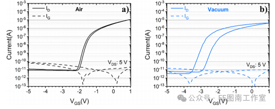
Figure 5. Dual-sweep semilog transfer characteristics of the β-Ga2O3 SFGT measured in (a) air and (b) vacuum at a pressure of 390 mTorr; for a device with WFIN of ∼90 nm.
doi.org/10.1021/acs.nanolett.5c03880
