Paper Sharing
【Member Papers】Co-doping improves memory characteristics in InSn-Ga₂O₃ detector via multiple impurity energy levels
日期:2025-10-15阅读:518
Researchers from the Nanjing University of Posts and Telecommunications have published a dissertation titled " Co-doping improves memory characteristics in InSn-Ga2O3 detector via multiple impurity energy levels " in Science China Technological Sciences.
Project Support
This work was supported by the Joints Fund of the National Natural Science Foundation of China (Grant No. U23A20349), the Young Scientists Fund of the National Natural Science Foundation of China (Grant Nos. 62204126, 62305171, 12104128, and 52402147), the Natural Science Foundation of Jiangsu Province (Grant Nos. BK20230361 and BK20241464), the Natural Science Foundation of Jiangsu Higher Education Institutions (Grant No. 23KJB510017), the Jiangsu Provincial Team of Innovation and Entrepreneurship (Grant No. JSSCTD202351), and the Postdoctoral Fellowship Program of CPSF (Grant No. GZC20233500).
Background
β-Ga₂O₃ has attracted significant attention for high-power electronics and optoelectronic devices due to its wide bandgap, excellent optoelectronic performance, and chemical stability. However, its low carrier concentration and high resistivity limit device performance. While single-element doping can enhance carrier density and tune optoelectronic properties, co-doping strategies further overcome solubility limits, reduce defect levels, improve conductivity and photoresponse, and introduce memory-like characteristics. In this work, InSn co-doped Ga₂O₃ thin films were epitaxially grown on c-plane sapphire substrates via PECVD, achieving bandgap modulation, increased carrier concentration, and enhanced photoresponse. Additionally, defect and surface-trapping effects prolong carrier lifetime, expanding the potential of Ga₂O₃ materials for optoelectronic synapses and image storage applications.
Abstract
In recent years, co-doping has gained widespread attention with the advantages of higher solubility, more carrier concentration, etc. Although more impurity energy levels will be introduced by co-doping, this can be in favor of appropriate application in the memory-effect device instead. Herein, the In and Sn co-doped gallium oxide (InSn-Ga2O3) film has been successfully grown on sapphire substrates using plasma-enhanced chemical vapor deposition technology. Compared with pure Ga2O3, InSn-Ga2O3 exhibits a significantly increased carrier concentration and numerous defects, and thus results in a slow carrier recombination process and a prolonged recovery time after illumination, which endows InSn-Ga2O3 with a certain memory function. Moreover, the first-principles calculation is utilized to analyze band structure evolution after the In and Sn co-doping, indicating the positive impact of multiple shallow impurity energy levels on improving conductivity and extending the recombination time of the photo-generated carriers in the InSn-Ga2O3 device. In all, this work demonstrates superior memory characteristics of Ga2O3 after co-doping operation and expands the potential applications of Ga2O3 in optoelectronic synapses and image storage devices.
Conclusion
In summary, we propose a previously unreported co-doped Ga₂O₃. The InSn-Ga₂O₃ films, fabricated using PECVD technology, demonstrate significant performance improvements. Compared with undoped Ga₂O₃, the optical bandgap decreases from 4.91 to 4.78 eV, accompanied by increases in both photocurrent and dark current, among which the dark current rises significantly by approximately five orders of magnitude. The carrier concentration is also noticeably enhanced. Through first-principles calculations, we analyzed the changes in energy bands and carrier concentration between pure Ga₂O₃ and InSn-Ga₂O₃, explaining their photoresponsive characteristics under 254 nm UV light. Furthermore, the large number of defects and surface states introduced in InSn-Ga₂O₃ slows down the carrier recombination process, resulting in a longer recovery time after illumination and endowing the material with certain memory functions. This research not only expands the application potential of Ga₂O₃ materials in optoelectronic devices but also provides a theoretical basis for the design and optimization of future materials. Subsequent studies could explore the effects of different doping combinations to achieve more efficient photodetection performance.
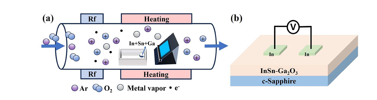
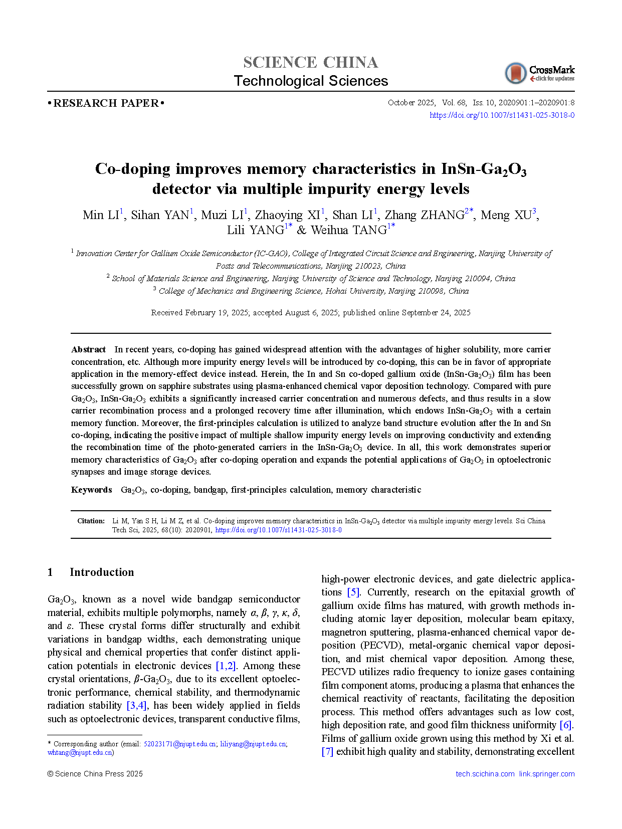
Figure 1 (a) PECVD system and deposition process of InSn-Ga2O3 films; (b) schematic diagram of InSn-Ga2O3 film.
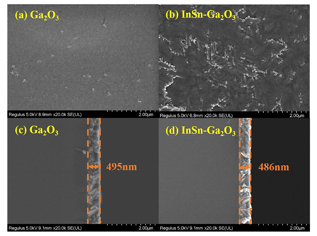
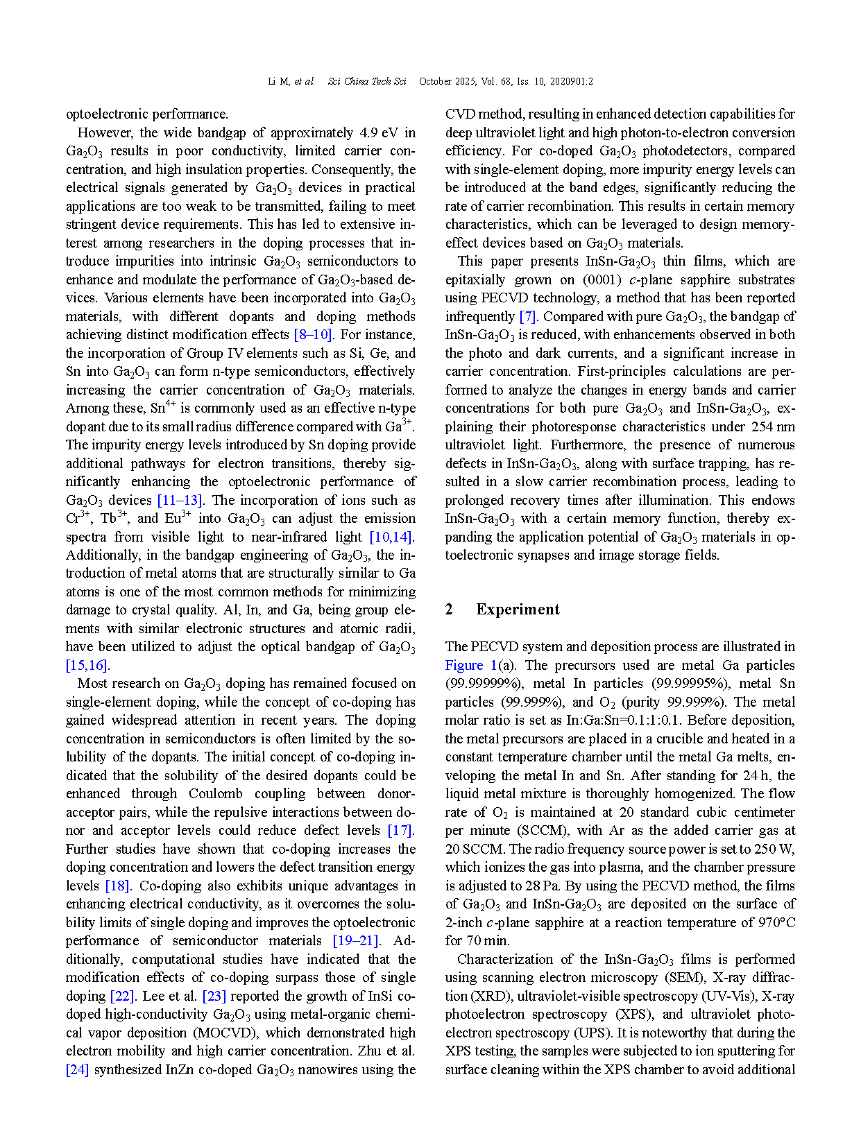
Figure 2 SEM surface images of (a) Ga2O3 and (b) InSn-Ga2O3; cross-sectional images of (c) Ga2O3 and (d) InSn-Ga2O3.
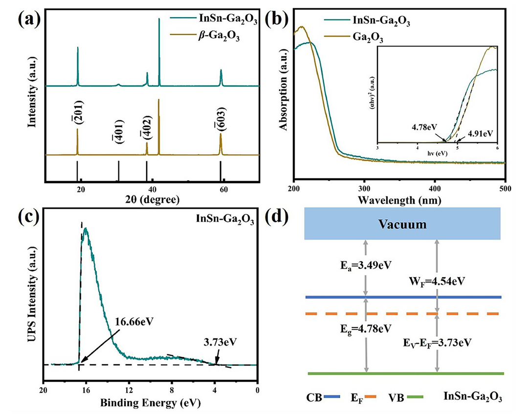
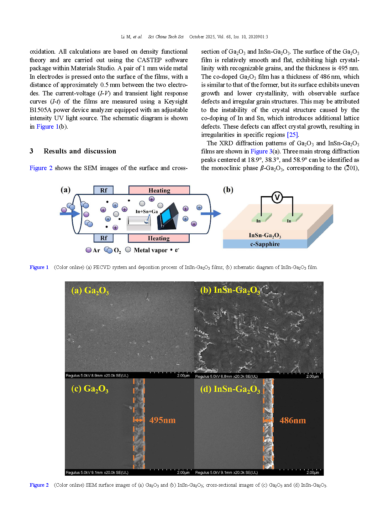
Figure 3 (a) XRD spectra and (b) UV-Vis absorption spectrum of Ga2O3 and InSn-Ga2O3 (inset: calculation of Eg); (c) UPS spectrum and(d) band diagram of InSn-Ga2O3.
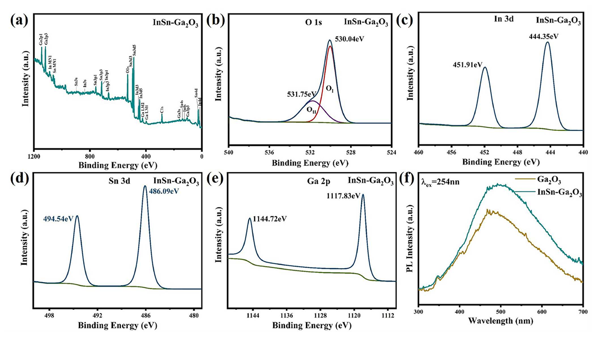
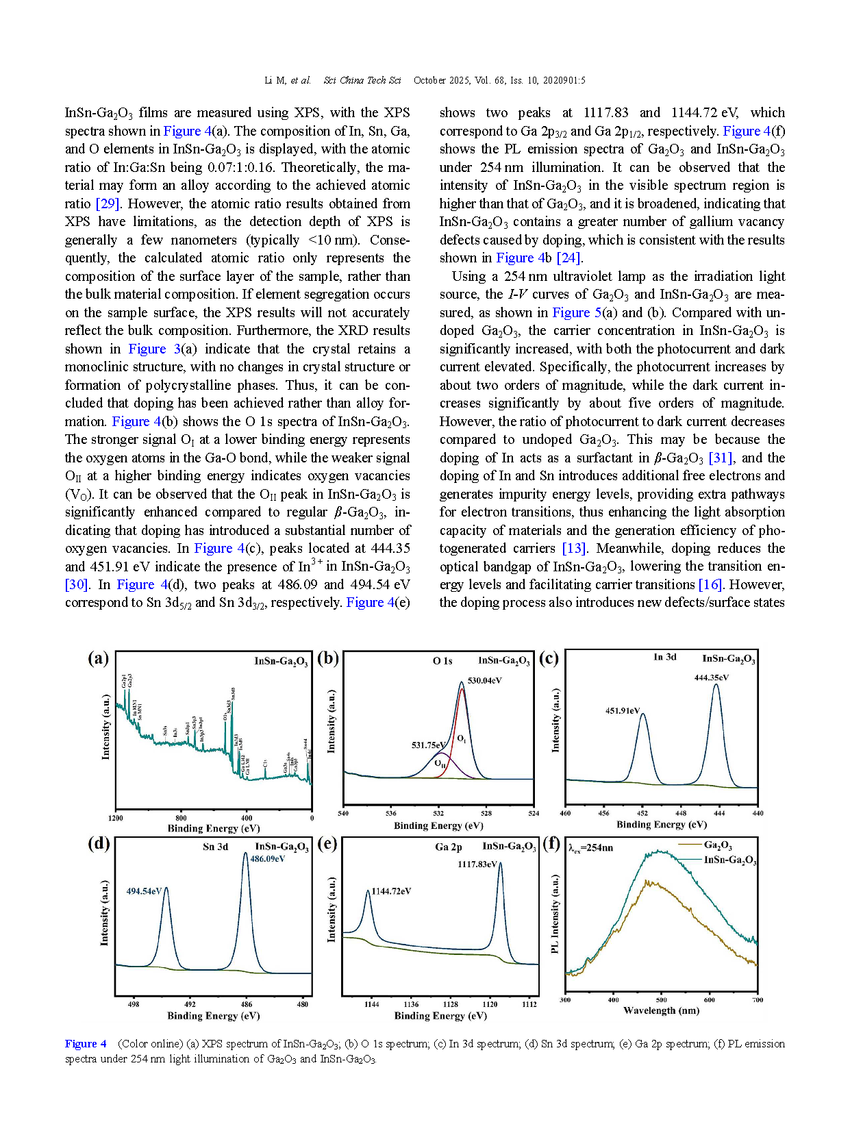
Figure 4 (a) XPS spectrum of InSn-Ga2O3; (b) O 1s spectrum; (c) In 3d spectrum; (d) Sn 3d spectrum; (e) Ga 2p spectrum; (f) PL emission spectra under 254 nm light illumination of Ga2O3 and InSn-Ga2O3.
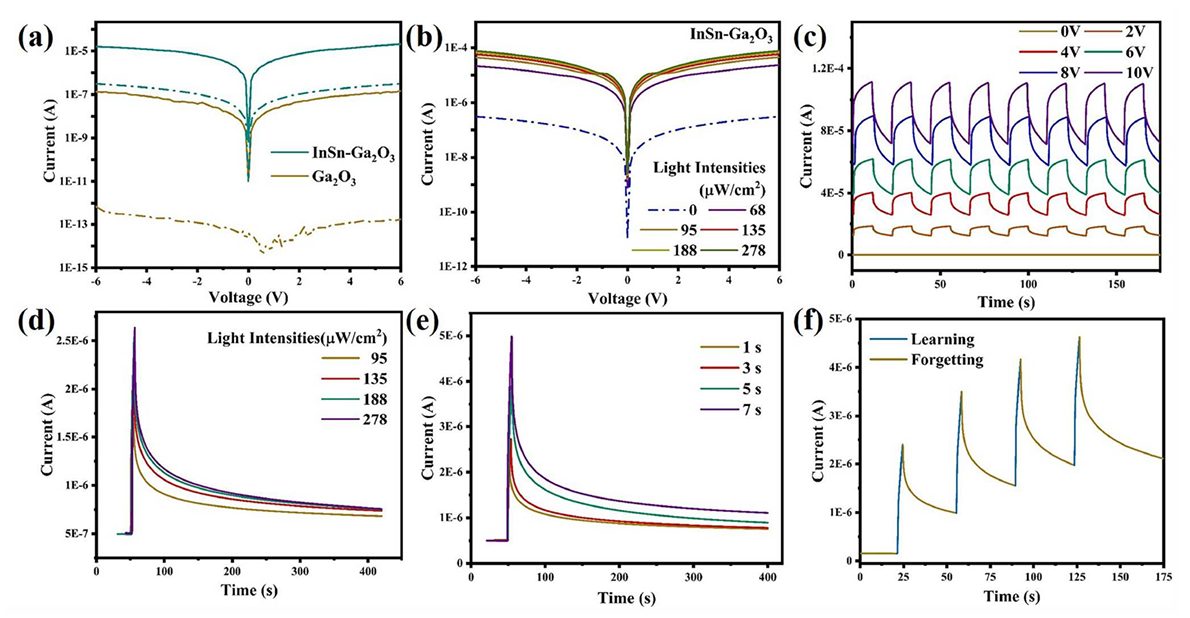
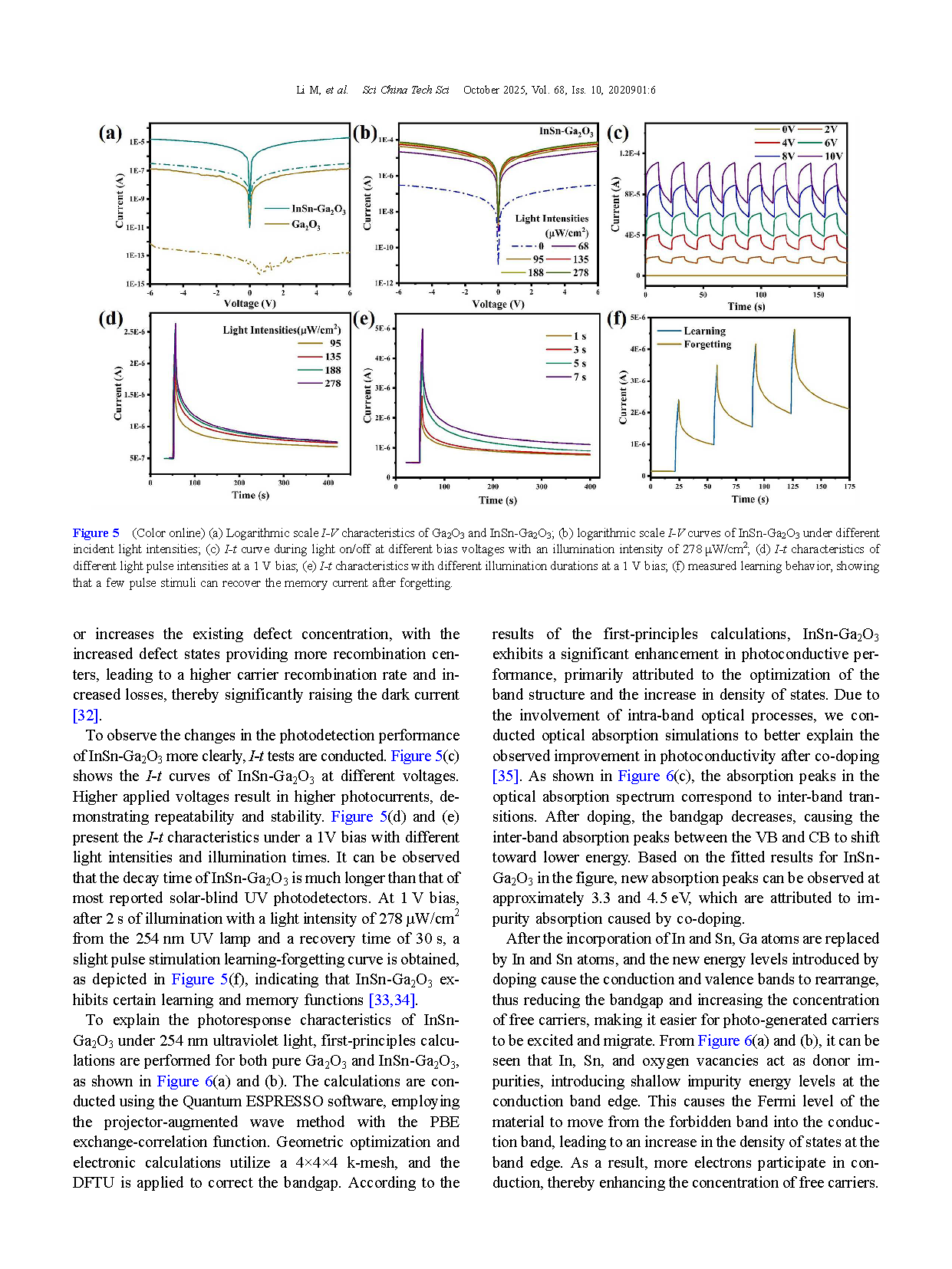
Figure 5 (a) Logarithmic scale I-V characteristics of Ga2O3 and InSn-Ga2O3; (b) logarithmic scale I-V curves of InSn-Ga2O3 under different incident light intensities; (c) I-t curve during light on/off at different bias voltages with an illumination intensity of 278 μW/cm2; (d) I-t characteristics of different light pulse intensities at a 1 V bias; (e) I-t characteristics with different illumination durations at a 1 V bias; (f) measured learning behavior, showing that a few pulse stimuli can recover the memory current after forgetting.
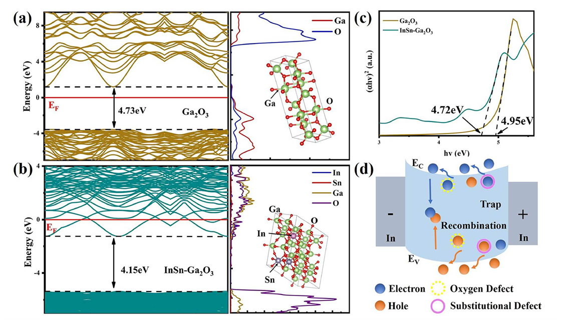
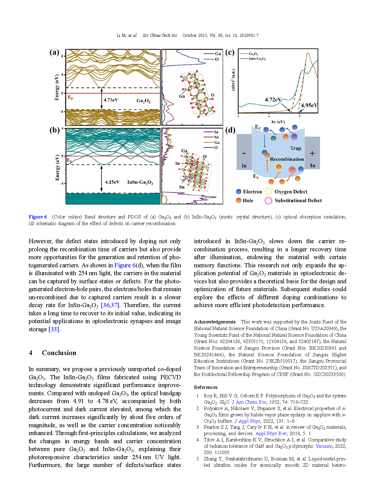
Figure 6 Band structure and PDOS of (a) Ga2O3 and (b) InSn-Ga2O3 (insets: crystal structure); (c) optical absorption simulation; (d) schematic diagram of the effect of defects on carrier recombination.
DOI:
doi.org/10.1007/s11431-025-3018-0