Paper Sharing
【Domestic Papers】Impact of different pumping and signal schemes on amplification performance of erbium-doped Ga₂O₃ waveguides
日期:2025-10-16阅读:507
Researchers from the Ningbo University have published a dissertation titled "Impact of different pumping and signal schemes on amplification performance of erbium-doped Ga2O3 waveguides" in Optics Express.
Project Support
This research supported by National Natural Science Foundation of China (62475126).
Background
Modern optical fiber communication demands high-speed, large-capacity data transmission, which drives the development of optical amplifiers to compensate for inherent signal losses. Erbium-doped fiber amplifiers (EDFA) leverage stimulated emission from erbium ions within the optical communication band and have been widely applied in commercial networks. With the rapid advancement of modern telecom systems, erbium-doped waveguide amplifiers (EDWA) have emerged as a preferred technology due to their miniaturization, low power consumption, and monolithic integration capability, making them suitable for datacom, access networks, coherent modules, and other applications requiring compact, low-power, and complex on-chip functionality. Host materials for Er-doped optical waveguide amplifiers typically require high transparency in the telecom band, high Er-ion solubility, and low phonon energy. Materials such as Si₃N₄, LiNbO₃, Al₂O₃, and Ta₂O₅ have been explored, often requiring ion implantation or chip bonding to achieve amplification. However, these methods are complex and challenging for large-scale industrial production. Gallium oxide (Ga₂O₃), as a fourth-generation semiconductor, exhibits excellent transparency from the ultraviolet to mid-infrared range, a high refractive index (~1.9), strong Er-ion solubility, and facile fabrication, making it a promising low-cost platform for Er-doped waveguide amplifiers compatible with standard semiconductor processing. Previous studies have demonstrated the feasibility of Er³⁺:Ga₂O₃ waveguides, achieving an on-chip gain of ~2.1 dB/cm at 1545 nm. Nevertheless, systematic comparisons of different pumping schemes (unidirectional vs. bidirectional) and signal sources on amplification performance are still lacking.
Abstract
Mode solutions simulations are employed to optimize the waveguide structure to enhance light interaction with rare-earth ions. Subsequently, an Er3+:Ga2O3 waveguide with an optimized structure is fabricated. The optical gain performance is characterized under bidirectional 980 nm pumping, using either a supercontinuum source or a single-wavelength laser as the signal. For a 0.5 cm long waveguide with a -32.4 dBm signal power and launched pump power of 59.4 mW, a net gain of 14.4 dB/cm at 1545 nm is obtained using the single-wavelength signal source. The maximum internal net gain reaches 23.2 dB/cm at a low signal power of -42 dBm, demonstrating the potential of amorphous gallium oxide thin films as a waveguide amplifier host material.
Conclusion
We designed a double-layer waveguide structure comprising Ta2O5 and Er3+:Ga2O3. The waveguide structure was optimized by simulating the overlap factor between the optical field and the rare-earth gain layer. We then prepared the corresponding films and waveguides. Amplification performance under different pumping methods and signal lights was measured in a waveguide with a propagation loss of 2.5 dB/cm at 1310 nm. For a 0.5 cm long waveguide under bidirectional pumping, an on-chip net gain of 7.2 dB/cm at 1545 nm was achieved using a supercontinuum signal source (-32.2 dBm), and this increased to 14.4 dB/cm while employing a single-wavelength laser (-32.4 dBm) as the signal source. Compared with earlier unidirectional pumping results, it can be found that, bidirectional pumping effectively enhances waveguide gain, and this can be higher if using a single-wavelength signal source. Notably, a maximum on-chip net gain of 23.2 dB/cm was achieved under a low single-wavelength input signal power of -42 dBm and a launched pump power of 59.4 mW. These results validate the potential of amorphous gallium oxide thin films as a host material for optical waveguide amplifiers.
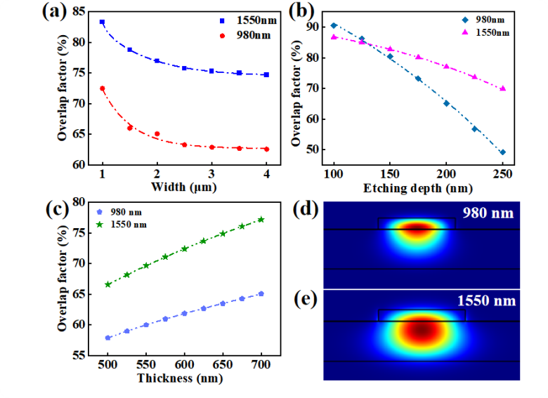
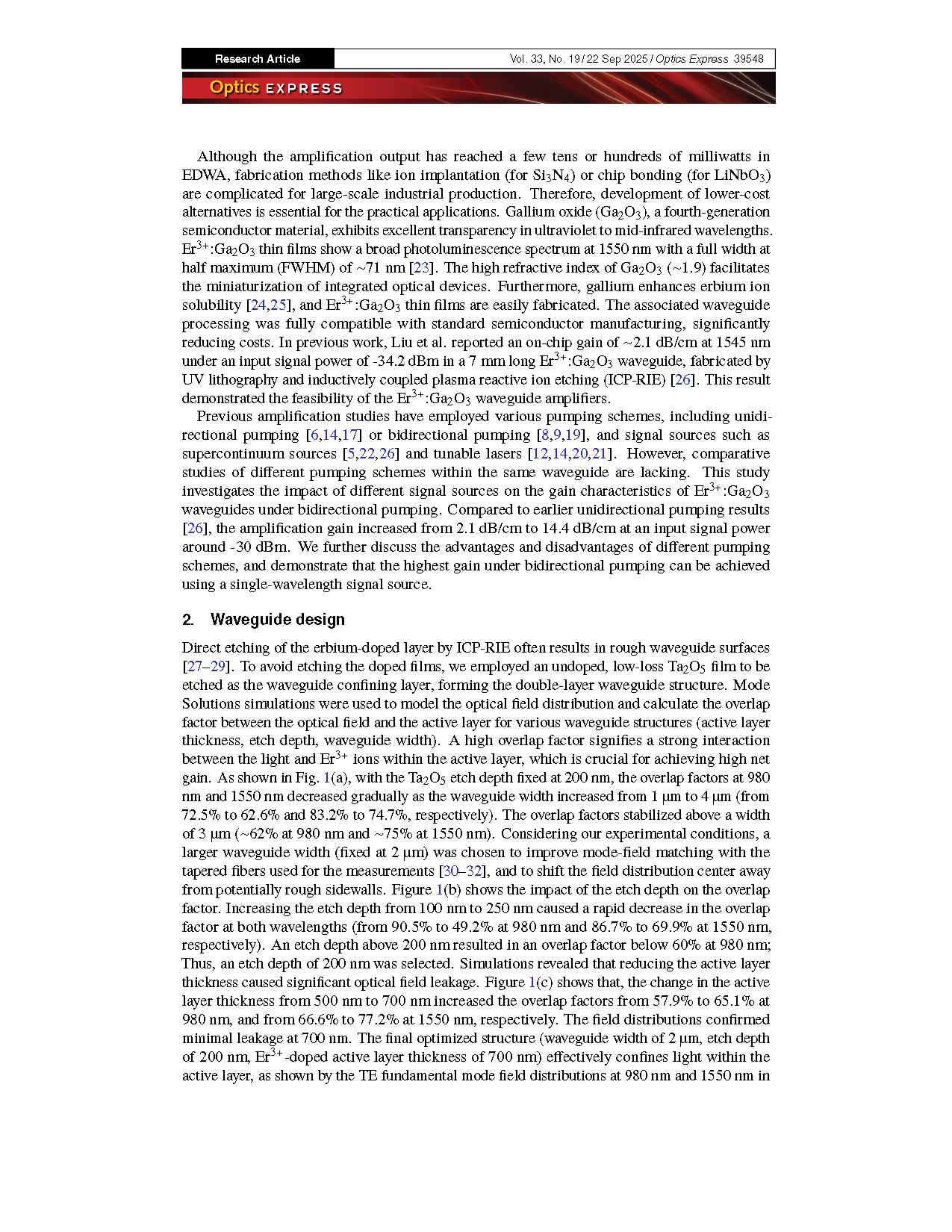
Fig. 1. (a) Evolution of the overlap factor with waveguide width; (b) Evolution of the overlap factor with etching depth; (c) Evolution of the overlap factor with thickness of Er3+:Ga2O3; (d) Optical field distribution at 980 nm; (e) Optical field distribution at 1550 nm.
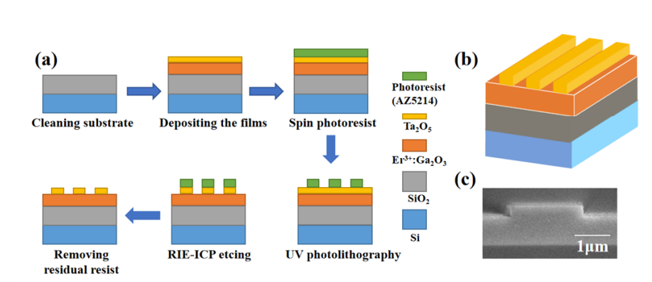
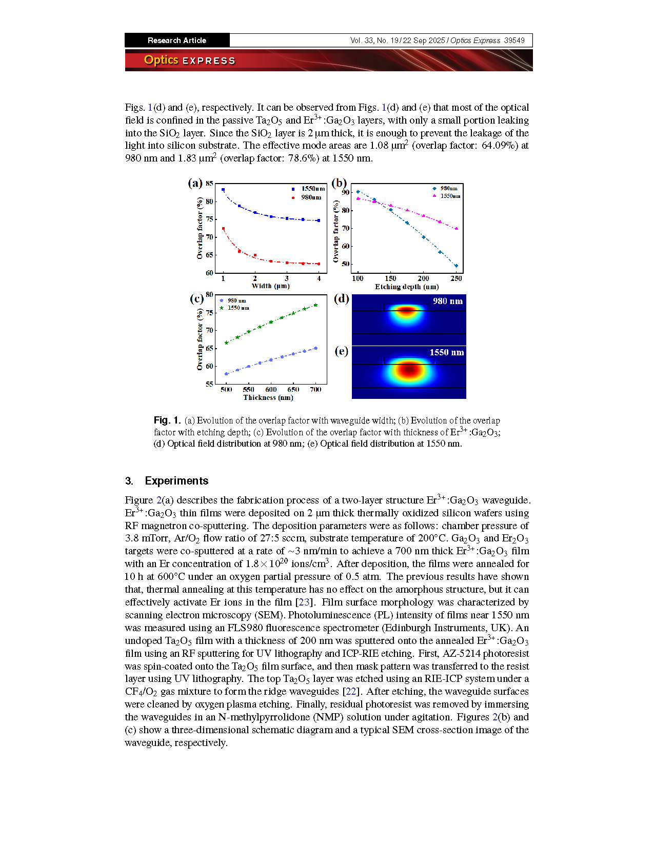
Fig. 2. (a) Process of double-layer structures of Er3+:Ga2O3 waveguide optical amplifier fabrication; (b) The 3-dimensional diagram of the device; (c) SEM cross-sectional image of the waveguide.
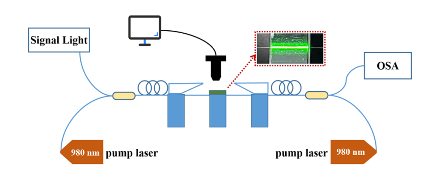
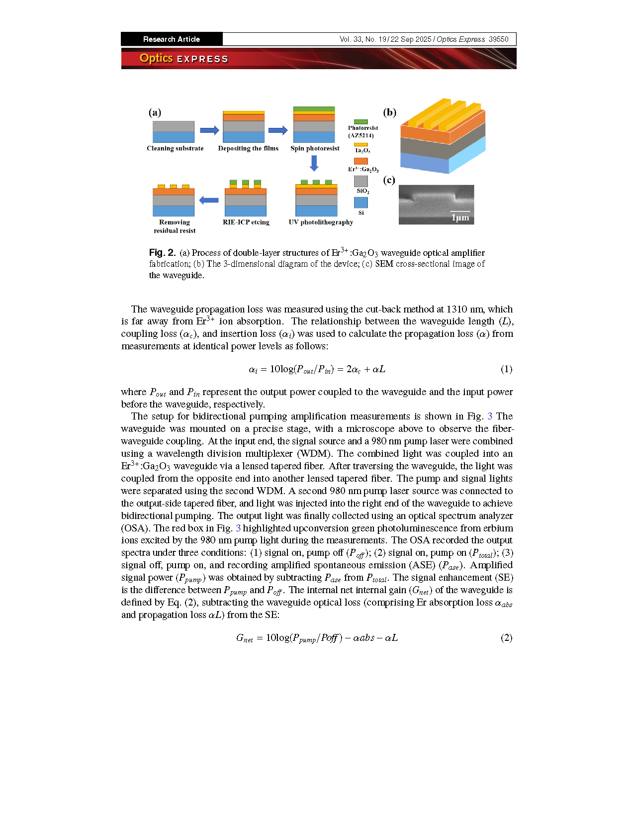
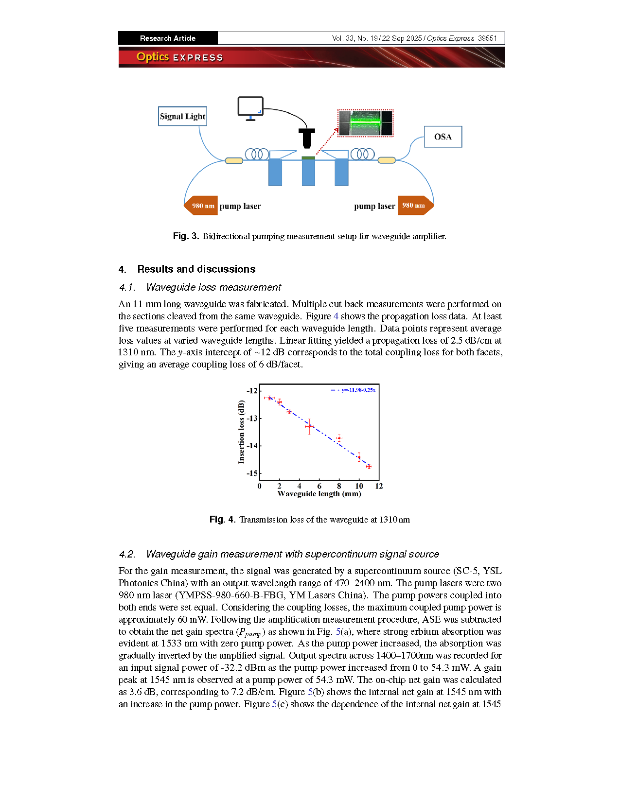
Fig. 3.Bidirectional pumping measurement setup for waveguide amplifier.
DOI:
doi.org/10.1364/OE.573078