


Member News
【Member News】Breaking News │ Garen Semiconductor Successfully Achieves High-Quality 6-Inch Gallium Oxide Homoepitaxial Growth
日期:2025-10-19阅读:561
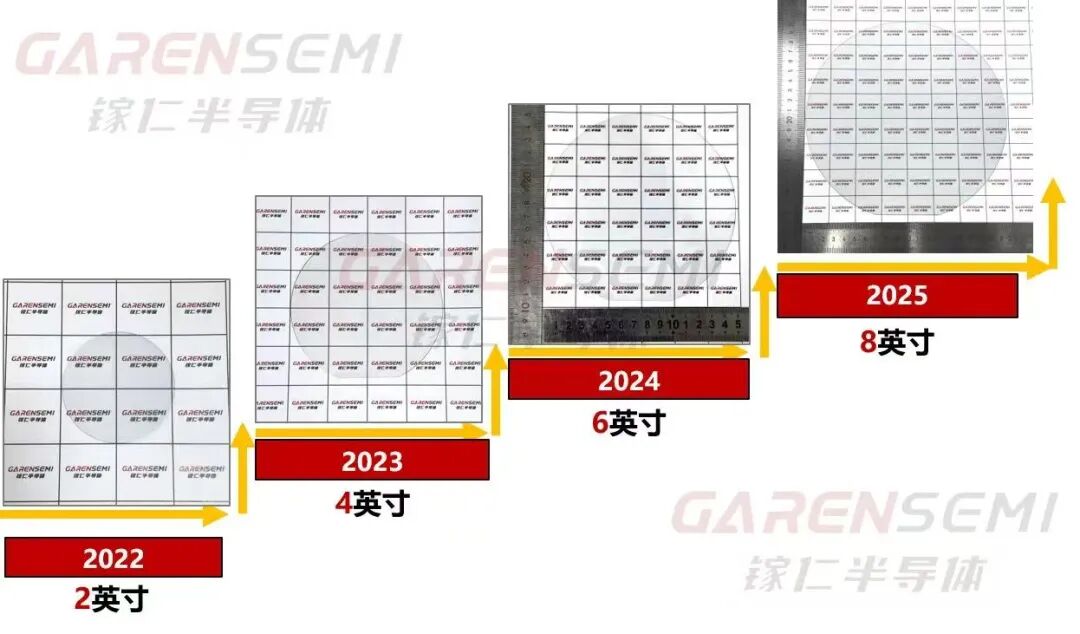
In September 2025, Hangzhou Garen Semiconductor Co., Ltd. (hereinafter referred to as “Garen Semiconductor”) officially announced a major breakthrough in epitaxy technology, successfully achieving high-quality 6-inch homoepitaxial growth of Gallium Oxide. This milestone marks a significant step in Garen Semiconductor’s development journey.
Inspection of the epitaxial wafers shows: the epitaxial layer thickness exceeds 10 μm with excellent uniformity, thickness variance σ < 1%; epitaxial quality is outstanding, with high-resolution XRD rocking curve full width at half maximum (FWHM) < 40 arcsec; carrier concentration in the epitaxial layer averages 1.8 × 10¹⁶ cm⁻³.
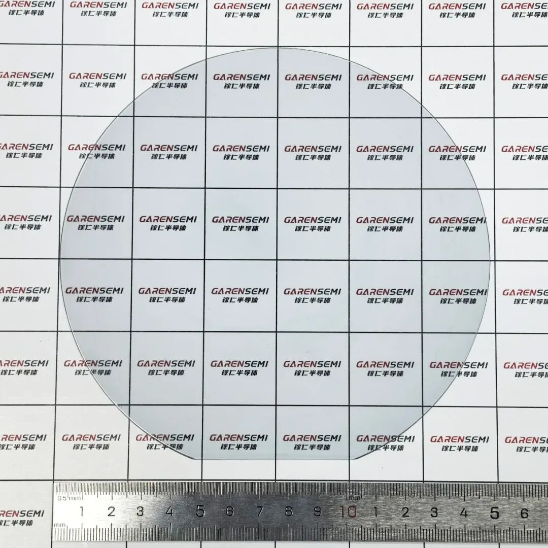
Figure 1: 6-inch Gallium Oxide Homoepitaxial Wafer by Garen Semiconductor
Outstanding Performance of Homoepitaxial Wafers
Infrared film thickness testing indicates that the average thickness of the 6-inch Gallium Oxide epitaxial layer exceeds 10 μm, with excellent uniformity (σ < 1%), demonstrating Garen Semiconductor’s precise process control in epitaxy.
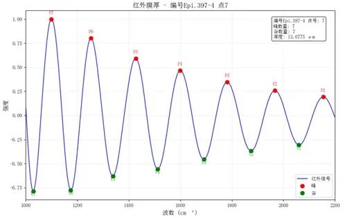
Figure 2: Infrared Reflective Film Thickness Measurement Curve
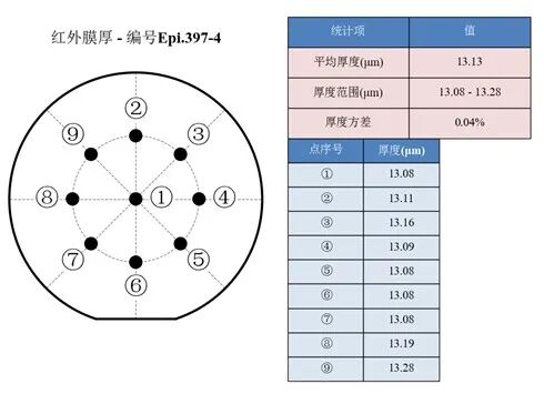
Figure 3: Distribution of Measurement Points and Corresponding Results
XRD testing shows a rocking curve FWHM of less than 40 arcsec, indicating high crystallinity and excellent lattice integrity of the epitaxial layer.
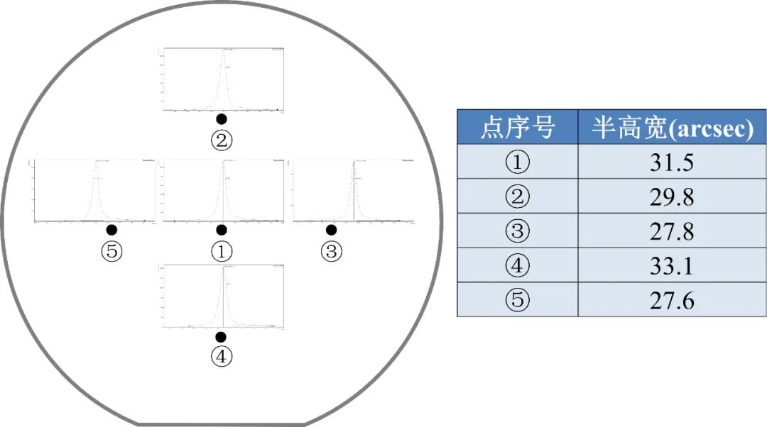
Figure 4: High-resolution XRD Rocking Curve and Corresponding Point Tests
Capacitance–Voltage (C–V) measurements reveal carrier concentrations ranging from 1.60 × 10¹⁶ cm⁻³ to 1.92 × 10¹⁶ cm⁻³, with a standard deviation of 6.08%, confirming good electrical uniformity of the epitaxial layer, suitable for high-voltage power device fabrication.
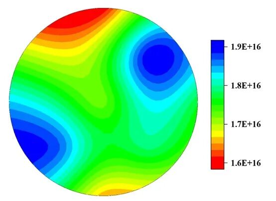
Figure 5: Carrier Concentration Distribution Map
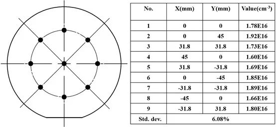
Figure 6: C–V Measurement Points and Corresponding Results
Significance of the 6-inch Homoepitaxial Breakthrough
Epitaxial growth is the process of “cloning” a high-quality thin film on a semiconductor substrate. Homoepitaxy, specifically performed on substrates of the same material, avoids lattice mismatch defects common in heteroepitaxy, making it the “optimal solution” for high-performance devices.
Garen Semiconductor’s achievement of 6-inch Gallium Oxide homoepitaxial growth is a milestone with profound significance:
1.Advantages of Homoepitaxy – The substrate and epitaxial layer being of the same material effectively eliminate lattice mismatch issues present in heteroepitaxy, enabling high-quality epitaxial layers. It also reduces thermal stress caused by differences in thermal expansion coefficients, thereby minimizing defects. Low defect density reduces electron scattering during transport, allowing power devices made from homoepitaxial material to approach the theoretical performance limits of Gallium Oxide, achieving lower energy loss, higher breakdown voltage, and improved reliability.
2.Advantages of 6-inch Size – A 6-inch wafer is the minimum size compatible with mainstream silicon-based semiconductor production lines. Achieving this size allows the epitaxial wafers to be compatible with most existing silicon-based equipment, significantly reducing downstream industrialization costs. Moreover, the larger size increases the number of devices per wafer. Combined with Garen Semiconductor’s proprietary casting technology, this further reduces the consumption of precious iridium, lowering costs substantially compared to 4-inch wafers.
Leading Innovation at Gallium’s Speed
Founded in September 2022, Hangzhou Garen Semiconductor is a technology-driven company specializing in the research, development, production, and sales of wide bandgap semiconductor materials and equipment, including Gallium Oxide.
The company leverages Zhejiang University’s National Key Laboratory of Silicon and Advanced Semiconductor Materials and the Hangzhou International Science and Technology Innovation Center, forming an R&D and production team with Academician Yang Deren of the Chinese Academy of Sciences serving as chief advisor. The R&D team pioneered the casting method for Gallium Oxide single crystal growth, achieving an 8-inch single crystal breakthrough, becoming the first industrial company worldwide to master this technology. The produced 8-inch Gallium Oxide single crystals have been certified by authoritative institutions to exhibit internationally leading performance.
Garen Semiconductor has also independently developed VB-method dedicated single-crystal growth equipment for Gallium Oxide, capable of maintaining the high-temperature, high-oxygen environment required for growth and enabling fully automated crystal growth, reducing manual intervention and significantly improving production efficiency and crystal quality.
