


Member News
【Member News】Fujia Gallium’s MOCVD Epitaxial Wafers Empower the Full-Link Integration of Gallium Oxide Power Devices
日期:2025-10-20阅读:647
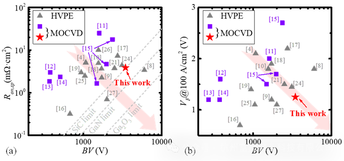
Recently, based on high-quality MOCVD thick-film epitaxial wafers provided by Hangzhou Fujia Gallium Technology Co., Ltd. (hereinafter “Fujia Gallium”), a research team from Fuzhou University successfully fabricated high-performance Gallium Oxide vertical power Schottky diodes. Among the publicly reported power Schottky diodes fabricated using MOCVD epitaxy, the PFOM performance achieved is the highest internationally (3.07 GW/cm²). From an industrial application perspective, among the publicly reported Gallium Oxide power Schottky diodes fabricated using both MOCVD and HVPE epitaxy, the devices exhibited the best overall performance in terms of conduction voltage and breakdown voltage. This work was published in Applied Physics Letters on September 2, 2025 (https://doi.org/10.1063/5.0276330
).
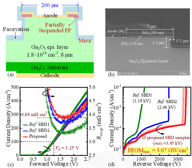
The research team employed device terminal structure design and process innovations to fabricate Schottky diode devices with partially suspended field plates. These modifications optimized the edge surface electric field distribution and reduced the electric field within the dielectric layer, effectively preventing premature breakdown and enhancing device breakdown voltage. The devices achieved a high breakdown voltage of 3.45 kV, a low specific on-resistance of 3.88 mΩ•cm², and a low on-voltage drop of 1.25 V.
Beyond terminal structure design and process improvements, the quality of the epitaxial layer—especially the carrier mobility of the epitaxial film—is critical for high-performance Gallium Oxide power devices. Epitaxial film mobility is closely related to conduction losses and directly reflects impurity scattering and defect density. Hall test samples prepared using the same MOCVD process as the epitaxial wafers in this work exhibited mobility of approximately 150 cm²/(V•s), strongly supporting the realization of high-performance Gallium Oxide power devices.
Subsequently, Fujia Gallium Industry achieved another breakthrough in MOCVD homogeneous epitaxial growth of Gallium Oxide. Testing by the national authoritative institution—the National Institute of Metrology, China—showed that Gallium Oxide homogeneous epitaxial wafers with thickness exceeding 10 μm achieved a mobility of 181.6 cm²/V•s. Device tape-out work for 6-inch Gallium Oxide homogeneous epitaxial wafers based on this process is currently underway.
Looking forward, Fujia Gallium Industry will provide high-quality Gallium Oxide epitaxial wafers to downstream scientific research and industrial users, support full-chain integration of high-performance Gallium Oxide power devices in China, and accelerate the rapid commercialization of high-voltage, high-power Gallium Oxide power electronic devices.
Product Introduction
Equipment:
The company has developed the world's first EFG equipment equipped with "one-click crystal growth", which can meet the growth requirements of 2-6-inch crystals. Currently, it has obtained 6 domestic authorized patents and 4 international authorized patents, and can provide equipment and supporting process packages.
The company independently developed fully automatic VB crystal growth equipment and was the first in China to break through the technical bottleneck of 6-inch single crystal growth, achieving the preparation of large-sized VB single crystal. At present, 6 domestic patents and 4 international patents are granted, and VB equipment and process packages can be provided according to customer requirements.
Taking into account the brittleness and easy cleavage characteristics of Gallium Oxide, the company has developed 2-6-inch Gallium Oxide single crystal substrate grinding and polishing equipment. According to customer needs, it can also provide mature grinding, polishing and cleaning process packages.
Single crystal and epitaxial wafer:
The company has established two enterprise standards and obtained ISO9001 quality system certification. It provides the market with 10mm to 6-inch Gallium Oxide single crystal substrates, 10mm to 6-inch MOCVD Gallium Oxide epitaxial wafer and 10×15mm MBE Gallium Oxide epitaxial wafer of various crystal directions.
About Hangzhou Fujia Gallium
Hangzhou Fujia Gallium Technology Co., LTD., founded on December 31, 2019, is the first "hard technology" enterprise registered by Hangzhou Institute of Optics and Fine Mechanics. With the vision of "Making the World Use Good Materials", the company focuses on the industrialization work of wide bandgap semiconductor Gallium Oxide materials. The core products include Gallium Oxide single crystal substrates, MOCVD epitaxial wafers, MBE epitaxial wafers, The VB method and EFG method crystal growth equipment, substrate grinding and polishing equipment, etc. provide systematic solutions for material development, accelerate the full chain connection of the ultra-wide bandgap Gallium Oxide industry, and promote the application of Gallium Oxide materials in power devices, microwave and radio frequency devices, and optoelectronic detection fields.The company's series of important achievements in the development of Gallium Oxide have been featured and reported by well-known media such as People's Daily, Xinhuanet, China Securities News, and The Paper.
Corporate Honors:
In 2022, it won the Zhejiang Province Science and Technology Small and Medium-Sized Enterprise; National High-Tech Enterprise in 2023; In 2024, it will be awarded as Hangzhou Enterprise High-Tech Research and Development Center and Zhejiang Special Small and Medium-Sized Enterprise. Obtain ISO9001 quality system certification in 2025 (No. 20225Q20294R0M) and 2024 Hangzhou “Rising Eagle” Enterprise. It undertook one Gallium Oxide project for the National Development and Reform Commission and participated in three national and provincial projects from the Ministry of Science and Technology, Zhejiang Province, and Shanghai. In addition, it has obtained 12 international patents authorized (6 in the United States and 6 in Japan), 40 domestic patents authorized, 3 trademark certification and registration of "Fujia Gallium", and 4 software copyrights (crystal growth control software of "one-click crystal growth").
