Paper Sharing
【Member Papers】Passivation engineering enhanced photodetection in β-Ga₂O₃ deep ultraviolet photodetectors
日期:2025-10-23阅读:569
Researchers from the Nanjing University of Posts and Telecommunications and Inner Mongolia University have published a dissertation titled "Passivation engineering enhanced photodetection in β-Ga2O3 deep ultraviolet photodetectors" in Physica Scripta.
Project Support
This work was supported in part by the National Key R&D Program of China under Grant 2022YFB3605404, and in part by the National Natural Science Foundation of China under Grant 62304113.
Background
Deep ultraviolet (DUV) photodetectors are of great importance in applications such as space communication, flame detection, ozone layer protection, and missile tracking. While materials like AlGaN, MgZnO, and diamond have been employed, β-Ga2O3, with its wide bandgap (>4.8 eV) and strong solar-blind UV response, has attracted particular interest. Advances in epitaxial techniques such as MOCVD, HVPE, MBE, and mist-CVD have enabled the growth of high-quality Ga2O3 films, yet device performance remains limited by oxygen vacancy defects and undesirable conductivity. Most β-Ga2O3 photodetectors to date adopt the MSM structure, whose responsivity under weak signals often falls short despite optimization of growth conditions and electrode materials. Efforts to improve performance through fluorine doping, UV-ozone treatment, and organosilicon passivation have shown limited effectiveness. Recently, the introduction of a passivation layer to form MISIM structures, particularly with Ga2O3 passivation, has demonstrated significant improvements, making it a promising direction for β- Ga2O3 photodetectors.
Abstract
β-Ga2O3 has gained significant attention for deep ultraviolet (DUV) photodetection applications due to its ultra-wide bandgap (>4.8 eV). However, surface and interface states have impeded the achievement of high responsivity in β-Ga2O3 photodetectors. In this study, an Al2O3 passivation layer is introduced to mitigate the recombination processes in β-Ga2O3 photodetectors. The optimized device, termed the metal-insulator-semiconductor-insulator-metal photodetector (MISIM PD), exhibits exceptional DUV photodetection performance. The responsivity, detectivity, photo-todark current ratio, and both static and dynamic characteristics of the MISIM PD are compared with those of a conventional metal-semiconductor-metal (MSM) architecture. The MISIM PD achieves increases of up to 264.18% in responsivity, 482.86% in detectivity, and 853.14% in photo-to-dark current ratio. The measured photocurrent linearity, photo-absorption, and response time indicate a reduction in recombination centers, attributed to the passivation effect of Al2O3. Additionally, DUV imaging with the MISIM PD further underscores the advantages of Ga2O3-based photodetectors.
Conclusion
In summary, we have successfully fabricated a MISIM structured β-Ga2O3 PD. The research findings demonstrate a significant enhancement in the photodetection performance of the device upon the introduction of an Al2O3 passivation layer. Under a bias of 10 V and 254 nm wavelength illumination, the MISIM PD exhibits a responsivity of 306.39 mA/W, a detectivity of 4.18×10¹³ Jones, and a photo to-dark current ratio of 6.51×10⁵. Compared to the non-passivated device, the responsivity, detectivity, photo-to-dark current ratio were increased by a maximum of 264.18%, 482.86%, and 853.14%, respectively. The photocurrent linearity, photo-absorption and switching measurement confirm that the notable performance enhancements are attributed to passivation engineering. Furthermore, the potential for DUV imaging applications of the MISIM PD was also examined, further emphasizing its promise in weak-signal detection.
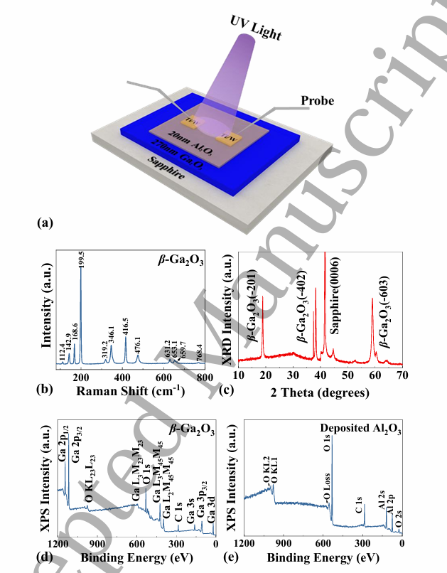
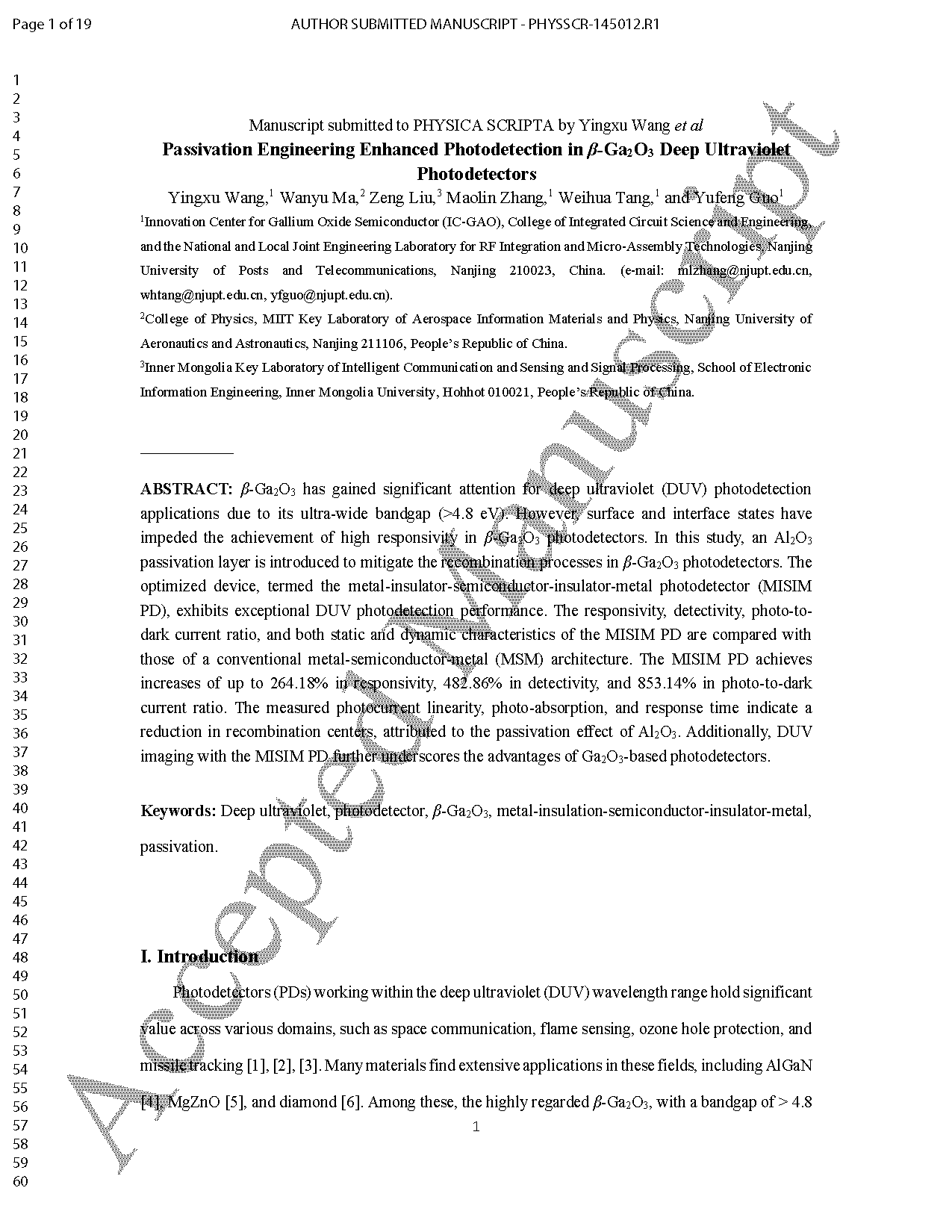
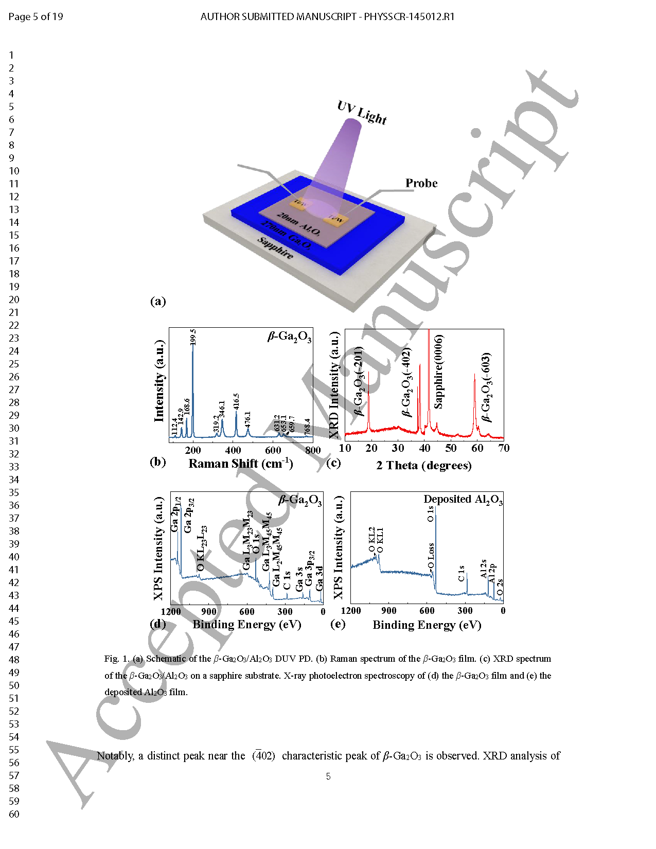
Fig. 1. (a) Schematic of the β-Ga2O3/Al2O3 DUV PD. (b) Raman spectrum of the β-Ga2O3 film. (c) XRD spectrum of the β-Ga2O3/Al2O3 on a sapphire substrate. X-ray photoelectron spectroscopy of (d) the β-Ga2O3 film and (e) the deposited Al2O3 film.
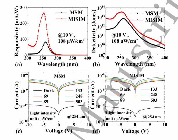
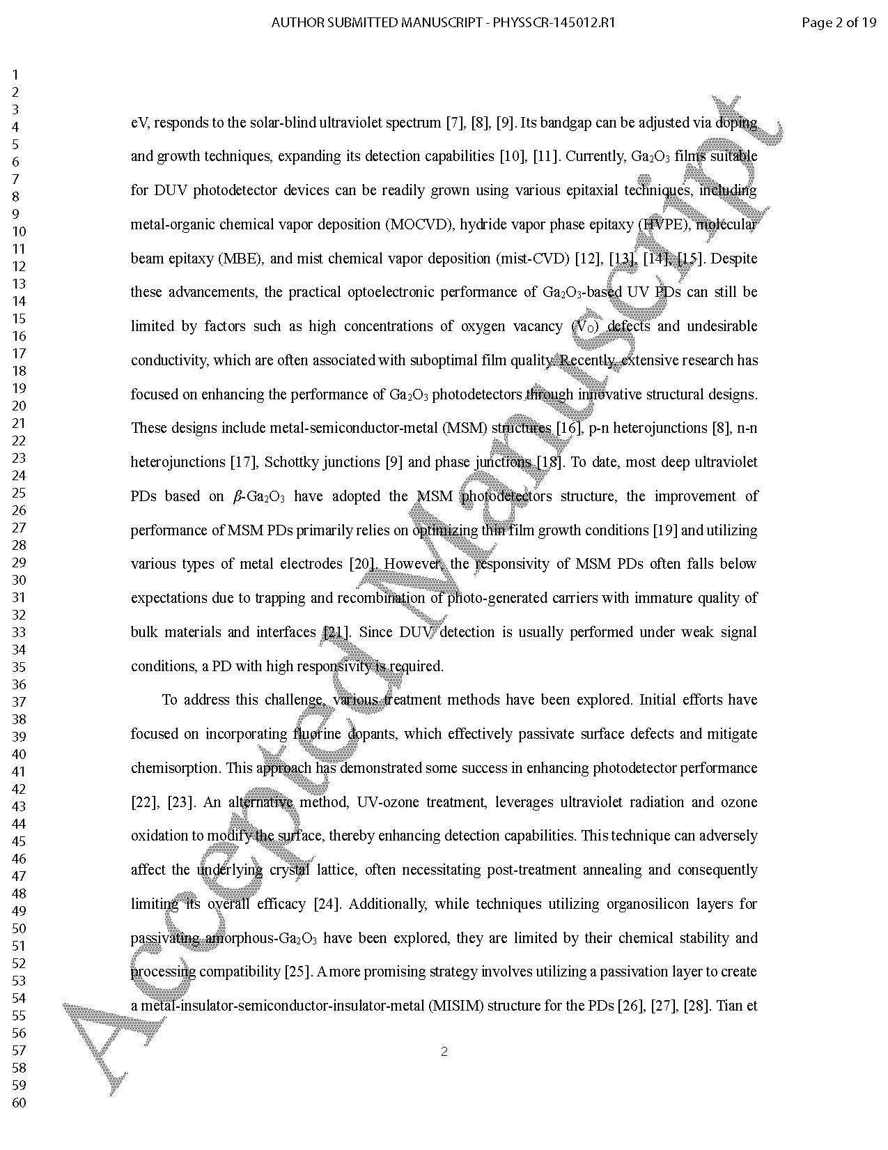
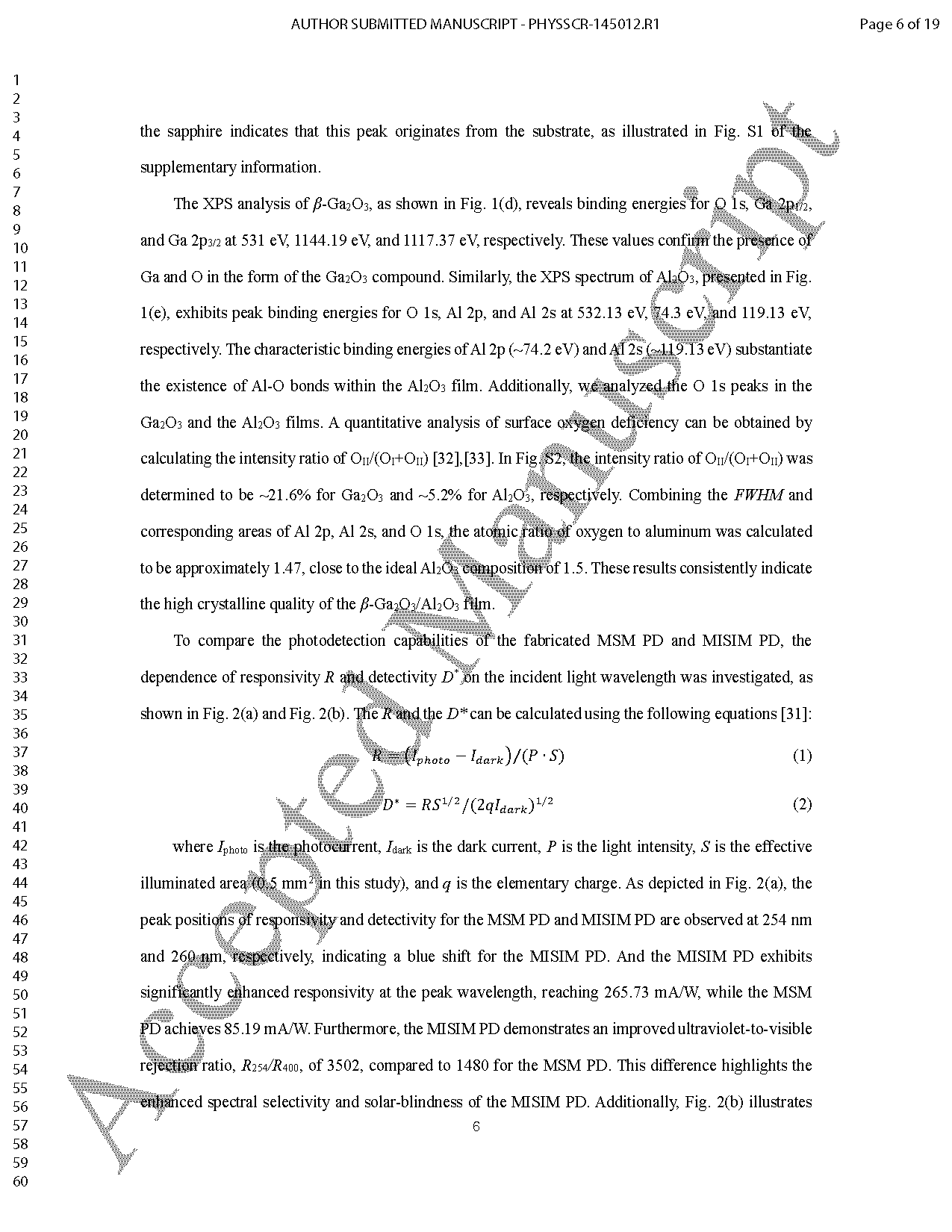
Fig. 2. (a) Responsivity and (b) detectivity dependency on wavelength of the MISIM and the MSM PDs. Measured I-V curves of (c) the MSM PD and (d) the MISIM PD.
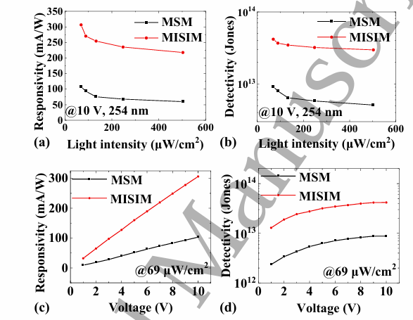
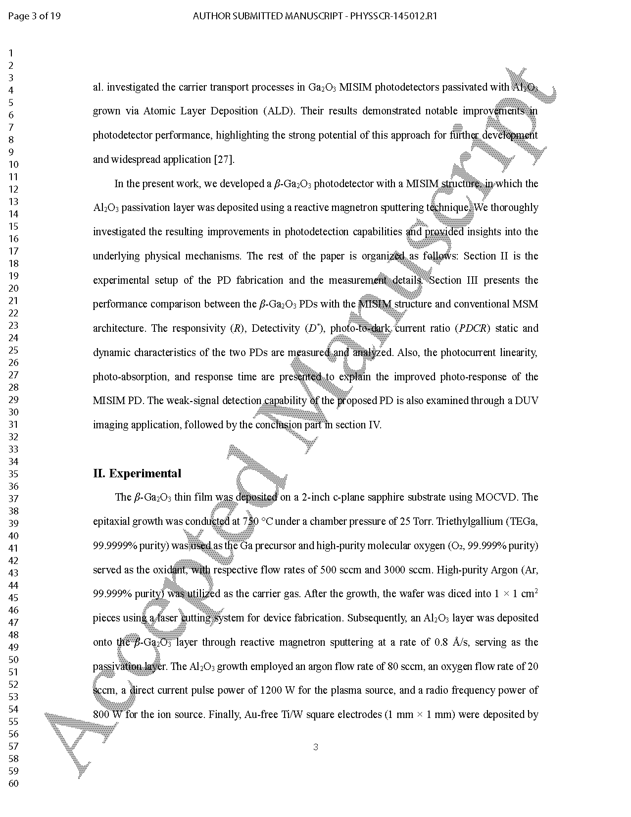
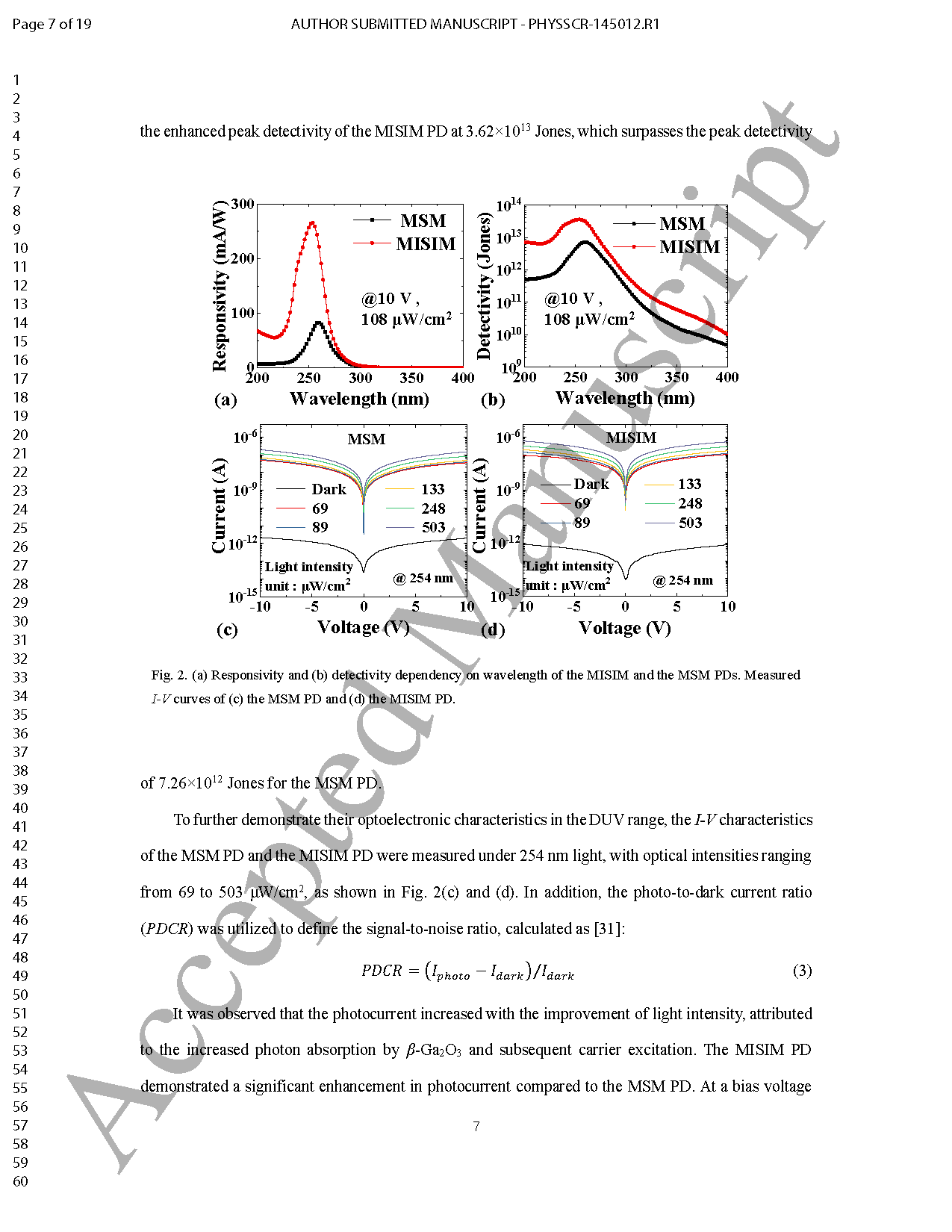
Fig.3. (a) Responsivity and (b) detectivity dependency on light intensity for both PDs. (c) responsivity and (d) detectivity of two PDs as a function of the bias voltage.
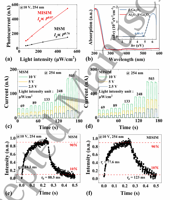
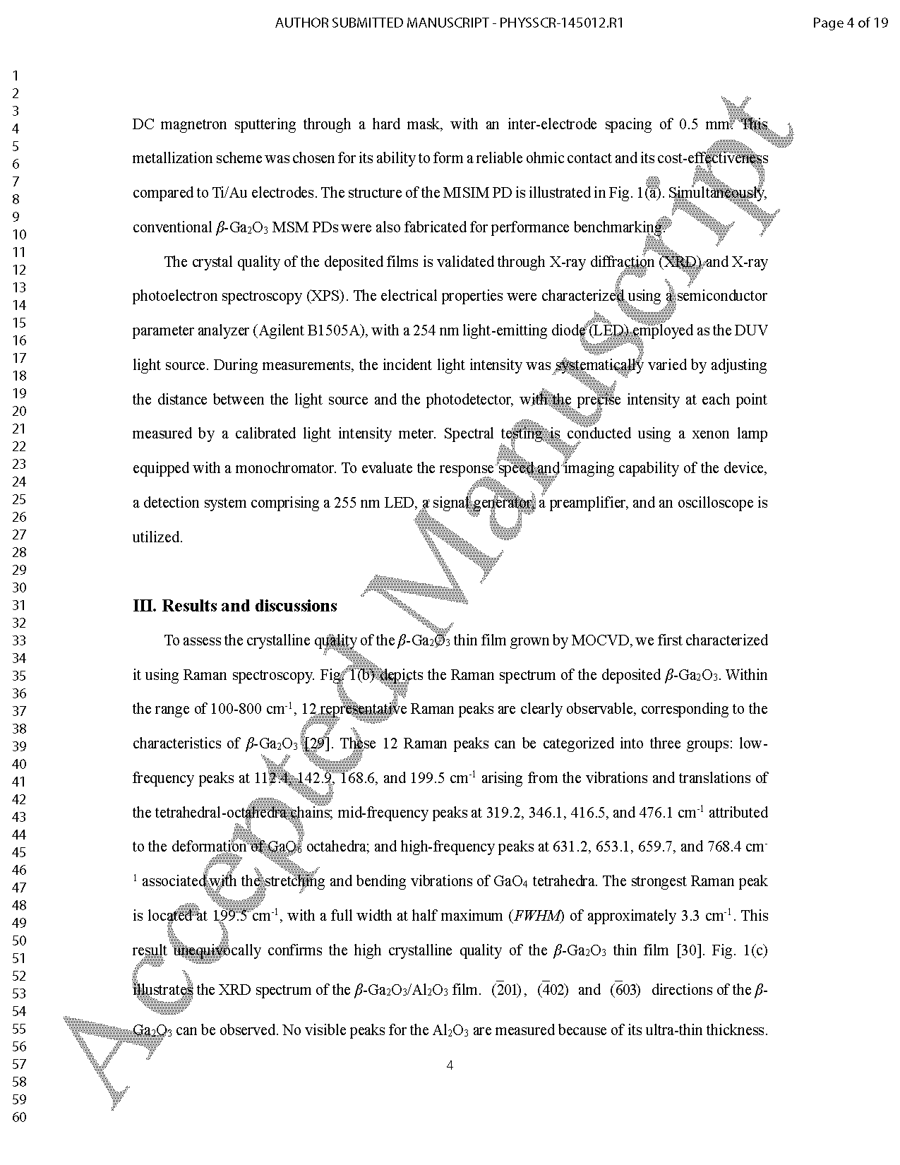
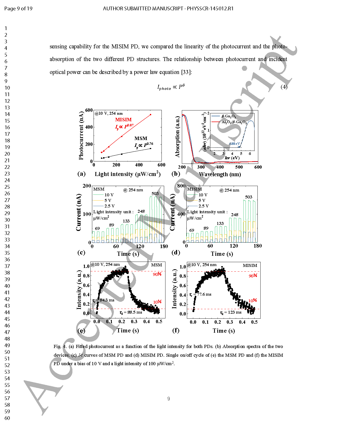
Fig. 4. (a) Fitted photocurrent as a function of the light intensity for both PDs. (b) Absorption spectra of the two devices. (c) I-t curves of MSM PD and (d) MISIM PD. Single on/off cycle of (e) the MSM PD and (f) the MISIM PD under a bias of 10 V and a light intensity of 100 μW/cm2.
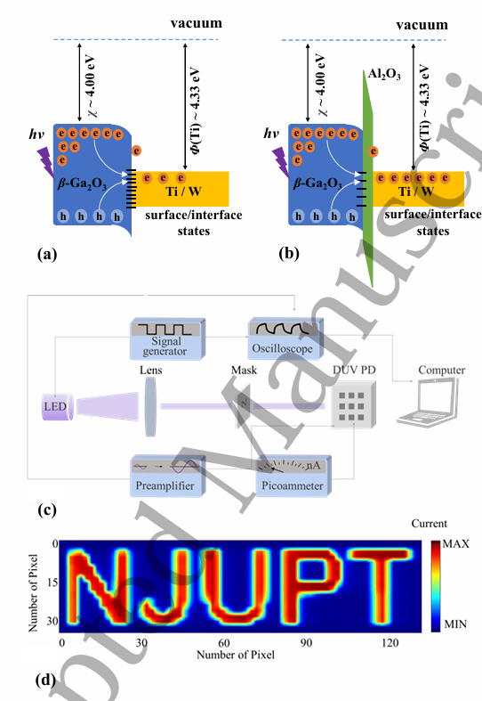
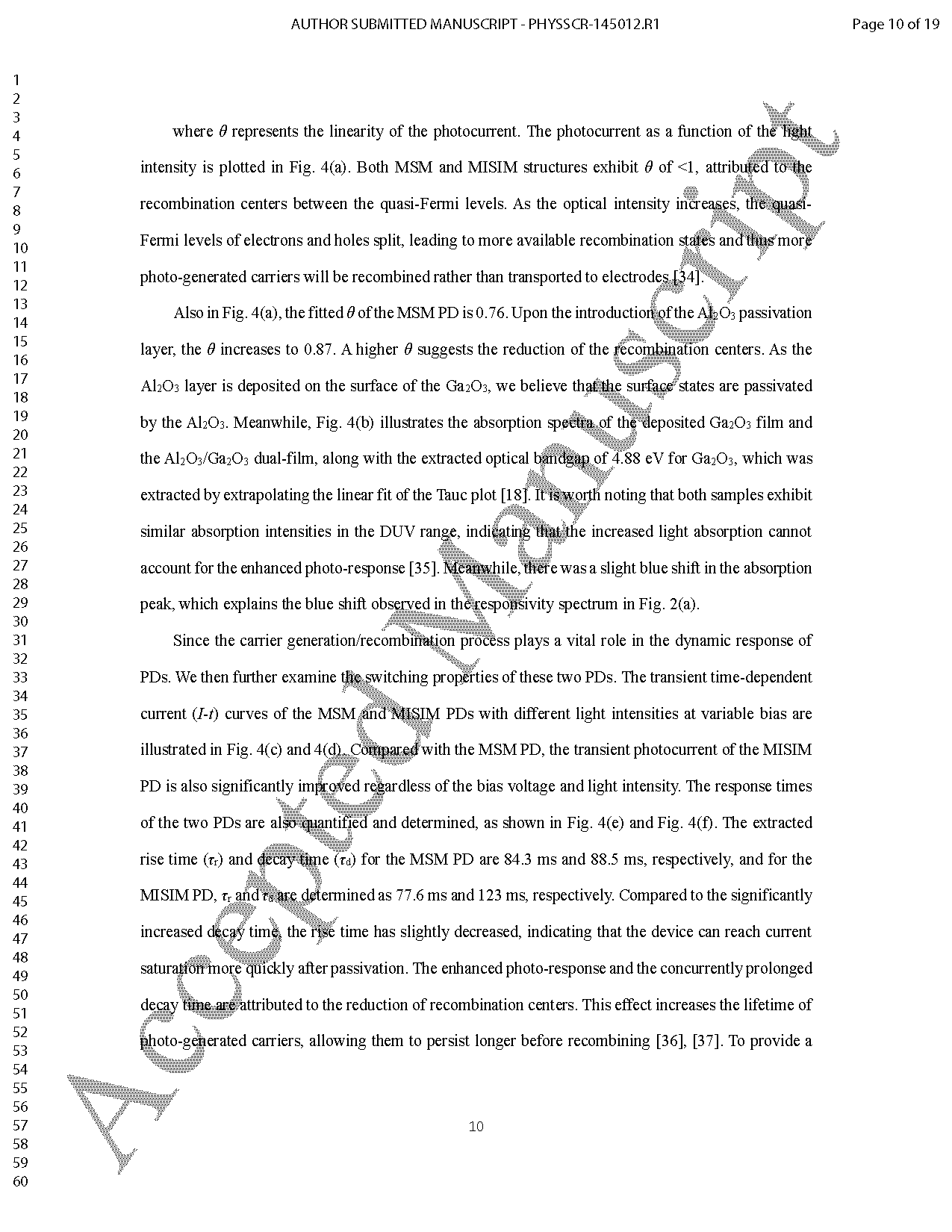
Fig. 5. The energy band diagram and schematics of (a) the MSM PD and (b) the MISIM PD. (c) Light path diagram of the DUV imaging system. (d) Imaging results with a “NJUPT” mask under 255 nm wavelength.
DOI:
doi.org/10.1088/1402-4896/ae04ac