Paper Sharing
【Member Papers】Catastrophic burnout mechanisms of NiO/β-Ga₂O₃ heterojunction diodes irradiated by 1.35 GeV high-energy heavy ions
日期:2025-10-23阅读:577
Researchers from the Harbin Institute of Technology and Nanjing University have published a dissertation titled "Catastrophic burnout mechanisms of NiO/β-Ga2O3 heterojunction diodes irradiated by 1.35 GeV high-energy heavy ions" in Applied Physics Letters.
Project Support
This work was supported by the National Key R&D Program of China (Nos. 2022YFB3605403 and 2023YFA1609000), the Jiangsu Provincial Key Research and Development Program of China (Nos. BE2023007-4 and BK20232045), the National Natural Science Foundation of China (Nos. 12075069, 12275061, 62304102, 62374084, 62234007, 62293522, U21A20503, and U21A2071), the State Key Laboratory of Space Environment Interaction with Matters, and the Guangdong Basic and Applied Basic Research Foundation under Grant No. 2025A1515011965. The authors would like to thank the Space Environment Simulation Research Infrastructure (SESRI) and the Frontiers Science Center for Matter Behave in Space Environment of Harbin Institute of Technology for providing irradiation support.
Background
Ultra-wide bandgap beta-phase gallium oxide (β-Ga2O3) has attracted significant interest in aerospace electronics applications due to its exceptional material properties, including a high threshold displacement energy and a large breakdown electric field (E-field). In the space radiation environment, heavy ions originating from high-energy collisions of cosmic rays, solar flares, and coronal mass ejections pose a critical threat by accelerating device degradation and even causing catastrophic burnout. The linear energy transfer (LET), representing the energy deposited by heavy ions at a specific depth in the device, is a crucial metric outlined in the JEDEC standard for evaluating radiation hardness. Devices typically require tolerance to LET values as high as 75 MeV·cm2/mg. Achieving such exposure involves high-energy heavy ions like Ta ions, which are available only at a few global irradiation facilities. Limited access to these resources restricts a comprehensive understanding of the irradiation response and durability of the emerging Ga2O3 power devices, leaving this area of research still in progress.
Abstract
Ultra-wide bandgap beta-phase gallium oxide (β-Ga2O3) power devices hold great promise in space applications; however, their intrinsic vulnerability to heavy ion irradiation, particularly defect behavior and catastrophic burnout mechanisms, remains largely unexplored. By performing bias voltage-dependent multiple rounds of statistical experiments with 1.35 GeV high-energy Ta ion irradiation, this work identifies electron and hole traps before burnout in NiO/β-Ga2O3 heterojunction diodes (HJDs), among which the introduced hole trap H2 (EV + 0.6 eV, 2.9 × 1013 cm−3) is revealed to dominate the irrecoverable leakage degradation associated with device damage by deteriorating the junction barrier. This trap in Ga2O3 is attributed to the electron energy loss along the ion incidence trajectory based on the “thermal spike” physics theory, possibly resulting in a localized amorphous latent track. Beyond device damage, the catastrophic burnout in irradiated HJD is identified in two distinct regions: Region I (p-NiO/n−-Ga2O3) dominated by trap-assisted electric field breakdown, and Region II (n−-Ga2O3/n+-Ga2O3) characterized by thermally driven damage from charge accumulation. Additionally, thermal effects also impact the active area of Region I along the carrier dissipation pathway. These findings provide insight into the damage and failure physics of β-Ga2O3 devices under heavy-ion strikes and inform strategies for improved irradiation hardness.
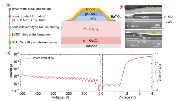
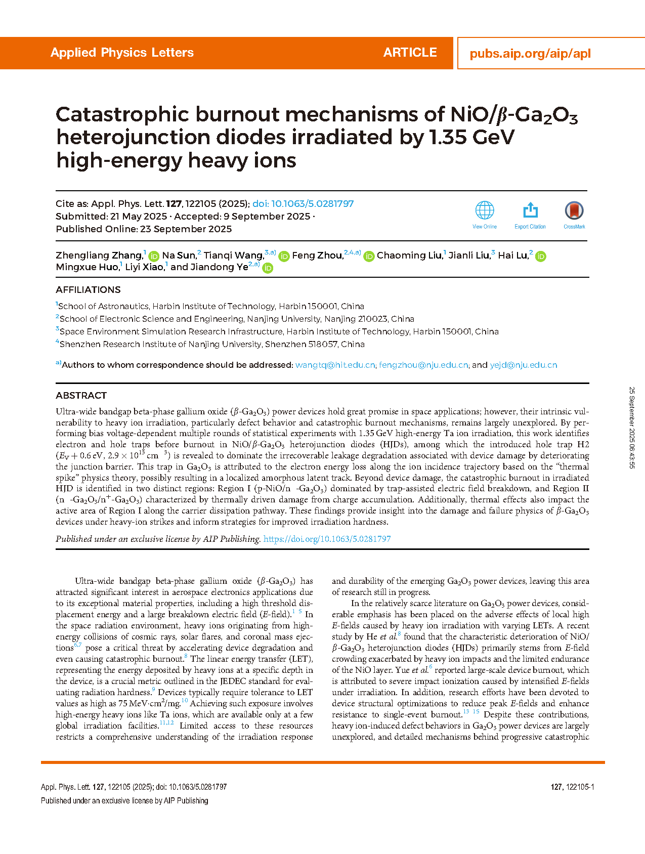
FIG. 1. (a) Process flow diagram and schematic structure of NiO/β-Ga2O3 HJD. (b) Cross-sectional SEM images of the fabricated device. (c) Forward and reverse I–V characteristics of the fabricated HJD before heavy ion irradiation. The current oscillation in the reverse leakage curve is due to instrumental measurement limitations.
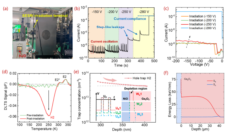
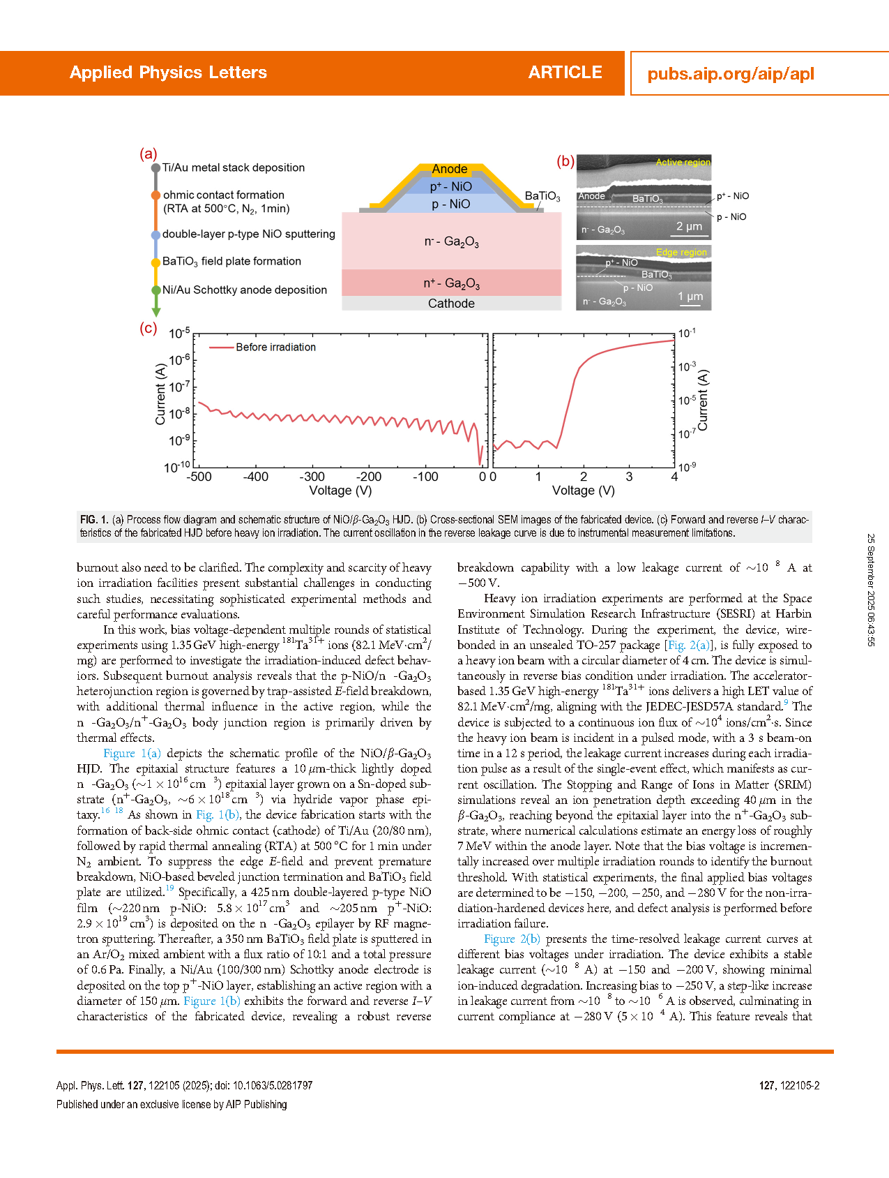
FIG. 2. (a) SESRI heavy ion irradiation experiment terminal and device under test. (b) Time-resolved leakage current curve under ion incidence with a heavy ion beam pulse of 3 s and a period of 12 s. (c) Leakage curves of post-irradiation HJD at different bias voltages. (d) DLTS spectra for devices before and after irradiation at -250 V (with UR = 5 and UP = 0.1 V). (e) The concentration of hole trap H2 as a function of depth within β-Ga2O3. (f) Sn and Se characteristic curves simulated by SRIM program
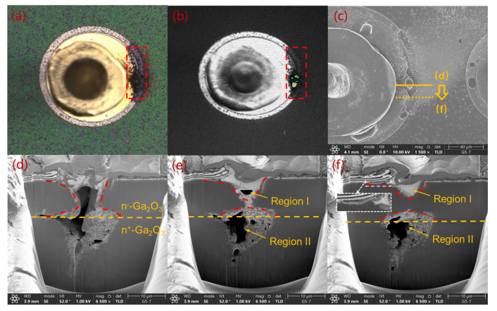
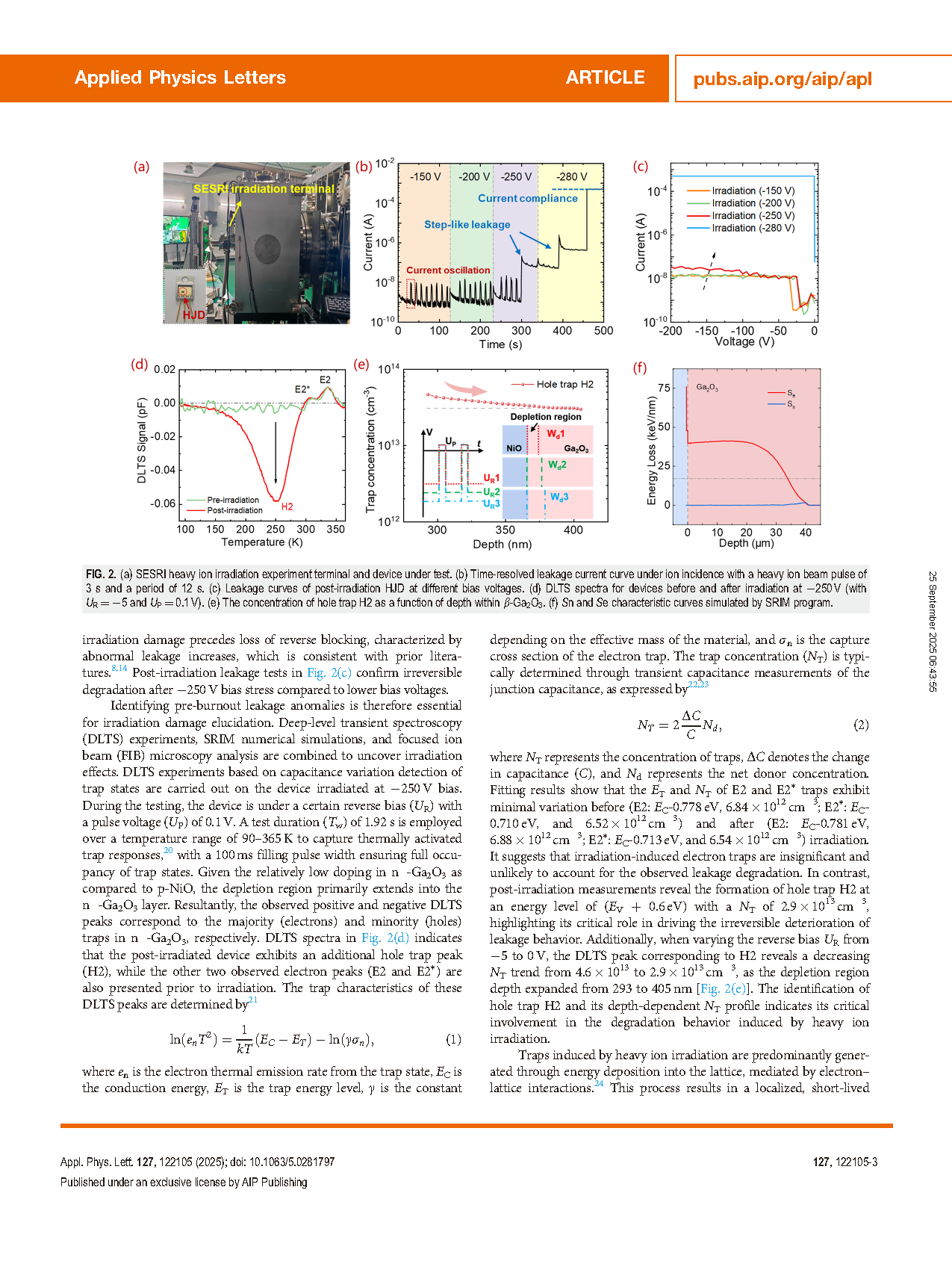
FIG. 3. (a) Optical photograph of catastrophic burnout of the irradiated HJD. (b) Emission microscopy image revealed distinct high-intensity emission sites that correlate with localized damage regions. (c) Cross-sectional cuts extending from the device center to its periphery, and the corresponding slice images (d)–(f). Evidently, the burnt path extends through the entire epitaxial structure into the highly doped substrate, forming an hourglass-shaped profile, narrow in the mid-layer, while expanding toward the top and bottom regions. Progressively slicing toward the periphery [(e) and (f)] reveals that the burnout damage is mainly concentrated in the top p-NiO/n--Ga2O3 heterojunction region (Region I) and the bottom n--Ga2O3/n+-Ga2O3 body junction (Region II).
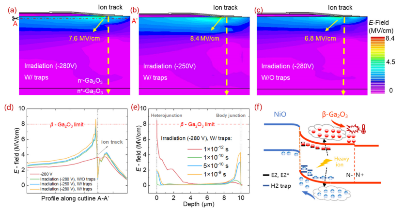
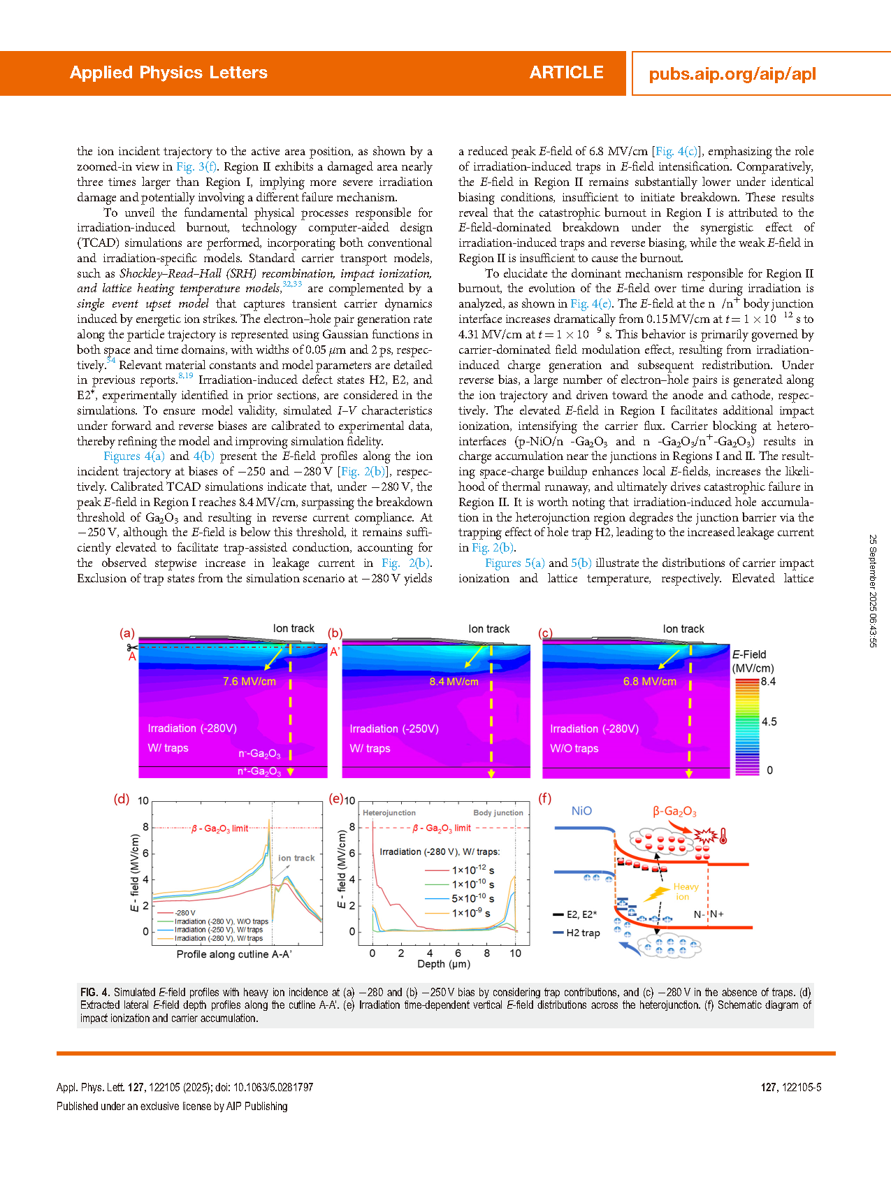
FIG. 4. Simulated E-field profiles with heavy ion incidence at (a) 280 and (b) 250 V bias by considering trap contributions, and (c) 280 V in the absence of traps. (d) Extracted lateral E-field depth profiles along the cutline A-A’. (e) Irradiation time-dependent vertical E-field distributions across the heterojunction. (f) Schematic diagram of impact ionization and carrier accumulation.
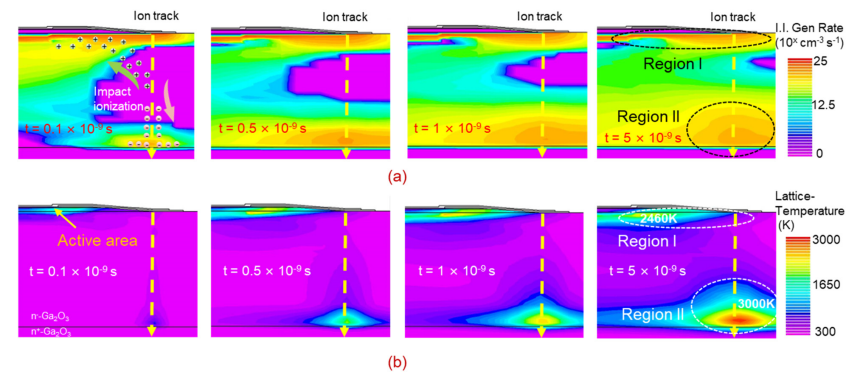
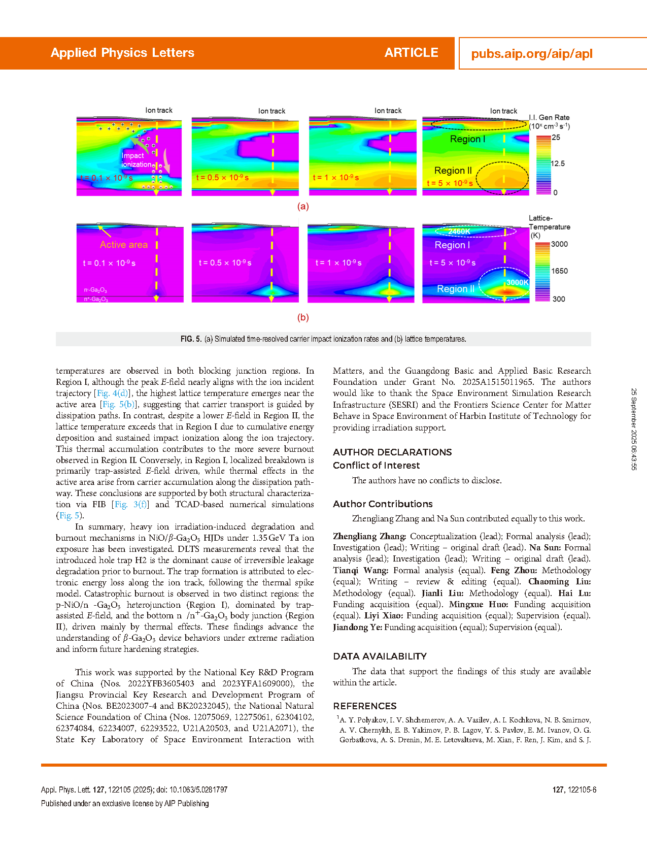
FIG. 5. (a) Simulated time-resolved carrier impact ionization rates and (b) lattice temperatures.
DOI:
doi.org/10.1063/5.0281797