Paper Sharing
【International Papers】Evidence for carrier compensation by gallium vacancies during annealing of highly Si-doped β-Ga₂O₃
日期:2025-10-24阅读:602
Researchers from the Cornell University have published a dissertation titled " Evidence for carrier compensation by gallium vacancies during annealing of highly Si-doped β-Ga2O3" in Journal of Applied Physics.
Background
Beta-phase gallium oxide (β-Ga2O3) has received attention in recent years due to its ultrawide bandgap (∼4.8 eV), high breakdown strength (∼8 MV/cm), and UV optical transparency. While other metastable polymorphs are also of interest, large single-crystals of the thermodynamically stable monoclinic β-Ga2O3 phase can be grown from the melt, facilitating rapid transition to commercial applications. For these reasons, β-Ga2O3 has tremendous potential relative to other wide and ultrawide bandgap semiconductors.
While there are significant challenges with p-type doping, n-type β-Ga2O3 can be readily achieved with various donors, including Si, Ge, and Sn substituting on Ga sites, F and Cl substituting on O sites, and H on interstitial sites. Unintentionally doped (UID) bulk β-Ga2O3 has been measured with >1018 cm−3 carriers, which was initially attributed to intrinsic oxygen vacancies (VO2+) due to the material's conductivity dependence on PO2 (σ ∼ PO21/4). Annealing β-Ga2O3 under oxygen-rich ambients resulted in the formation of insulating layers, which could be largely reversed under subsequent low PO2 annealing, or minimized with a SiO2 cap present during annealing ambient.
Abstract
Net carrier densities in highly Si-doped β-Ga2O3 decrease during thermal annealing as a function of temperature, time, and PO2 for both in situ and implant-doped films. The mechanism for this loss has been attributed to the formation of gallium vacancies (VGa3−), which act as compensating acceptors and form passivating defect complexes. Samples doped above 3 × 1019 cm−3, annealed at the same temperature and PO2, ultimately approach a similar net carrier density of 1–3 × 1019 cm−3 (for 950 °C and PO2 < 2 × 10⁻⁷ bar) independent of the starting dopant concentration or doping method. These highly doped samples, metastable under these conditions, generate VGa3− to reach the steady state |ND − NA|, determined by the Fermi level. An activation energy of 1.6 ± 0.2 eV was observed for the rate of net carrier loss in high concentration in situ doped films. Scanning transmission electron microscopy and electrical results for implanted samples show that dopant activation, lattice recovery, and compensation are all active within the first minutes of annealing. Understanding the metastability of higher doping levels and VGa3− formation allows for the development of mitigation strategies to achieve highly Si-doped β-Ga2O3 by implant (8 × 1019 cm−3 with >70 cm2/V s mobility), including using the minimum required anneal time to achieve lattice recovery and dopant activation, reducing vacancy formation. Compensation initially limited full activation of deeper implants to 1 × 1020 cm−3; by protecting the free surface with a SiO2 cap during annealing, the activation efficiency doubled, and the mobility increased by 30%, highlighting the importance of controlling VGa3− formation and compensation.
Conclusions
Findings presented in this work support the hypothesis that the decrease in net carriers as a function of extended annealing time, observed in both in situ and implant Si-doped films, arises from the formation of compensating gallium vacancies, VGa3−, and associated passivating defect complexes. Under given PO2 and temperature anneal conditions, net carriers decrease to a common range independent of the starting doping density; these data show vacancies will continue forming until the energy barrier to generate more VGa3− is no longer surmountable. The rate and extent of this VGa3− generation depends on PO2, impacting the defect formation energies and the reaction equilibrium, and temperature, impacting formation kinetics and diffusion. This process exhibits an activation energy of 1.6 ± 0.2 eV, linked to surface VGa3− formation and vacancy diffusion. Doping levels below 3 × 1019 cm−3 show only limited deactivation (at 950 °C and PO2 < 2 × 10⁻⁷ bar) with no significant mobility change, likely associated with only vacancy-dopant complex formation at longer times. Net active carriers rapidly decrease in highly doped samples with a decrease in mobility, due to increased ionized acceptors compensating Si donors and increasing ionized impurity scattering. For implanted films at higher doping concentrations, the mobility shows only limited changes with anneal time due to masking of the vacancy compensation at short times by lattice recovery processes. The use of a capping layer during annealing limits vacancy formation, enabling doubled activation to higher metastable net carrier densities near 1 × 1020 cm−3 with a 30% increase in mobility. These results show that metastable heavily n-type doping within β-Ga2O3 is feasible by both in situ doping and ion implantation if the formation of gallium vacancies is minimized to prevent deactivation.
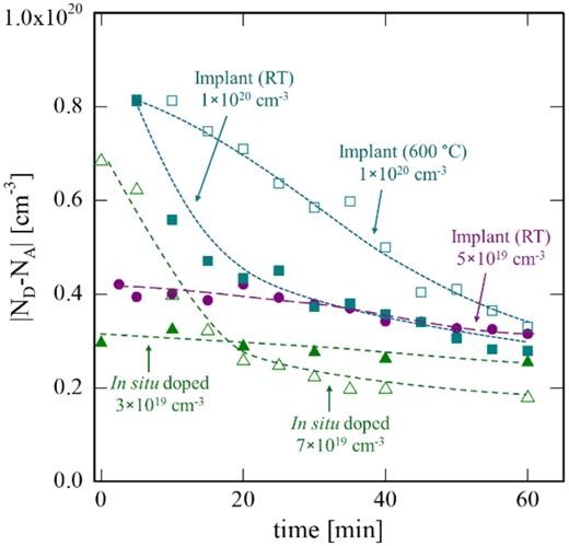
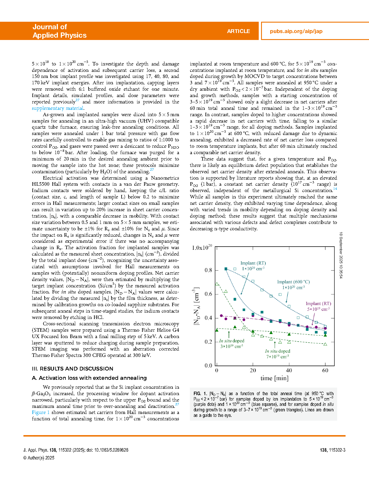
FIG. 1. |ND − NA| as a function of the total anneal time (at 950 °C with PO2 < 2 × 10⁻⁷ bar) for samples doped by ion implantation to 5 × 1019 cm−3 (purple dots) and 1 × 1020 cm−3 (blue squares), and for samples doped in situ during growth to a range of 3–7 × 1019 cm−3 (green triangles). Lines are drawn as a guide to the eye.
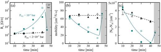
FIG. 2. Hall results of Rs (a), mobility (b), and |ND − NA| (c) for 5 × 1019 cm−3 implanted samples annealed at PO2 < 2 × 10⁻⁷ bar (black triangles) and PO2 = 10−4 bar (blue squares). Each anneal condition was tested with two samples to check repeatability, indicated with filled and open symbols of the same shape and color. High PO2 samples (blue) were electrically recovered with a 5-min anneal under the low PO2 conditions, as shown in the shaded gray area and marked with blue arrows. Lines are drawn as a guide to the eye.
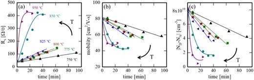
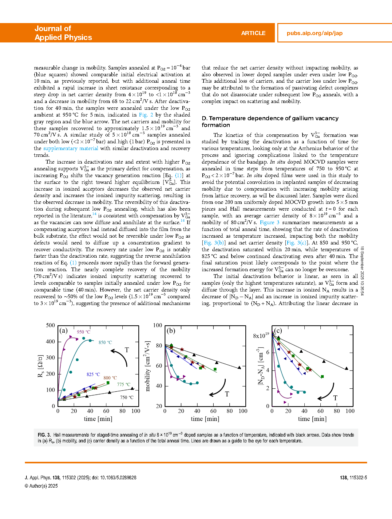
FIG. 3. Hall measurements for staged-time annealing of in situ 8 × 1019 cm−3 doped samples as a function of temperature, indicated with black arrows. Data show trends in (a) Rs, (b) mobility, and (c) carrier density as a function of the total anneal time. Lines are drawn as a guide to the eye for each temperature.
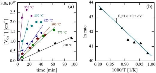
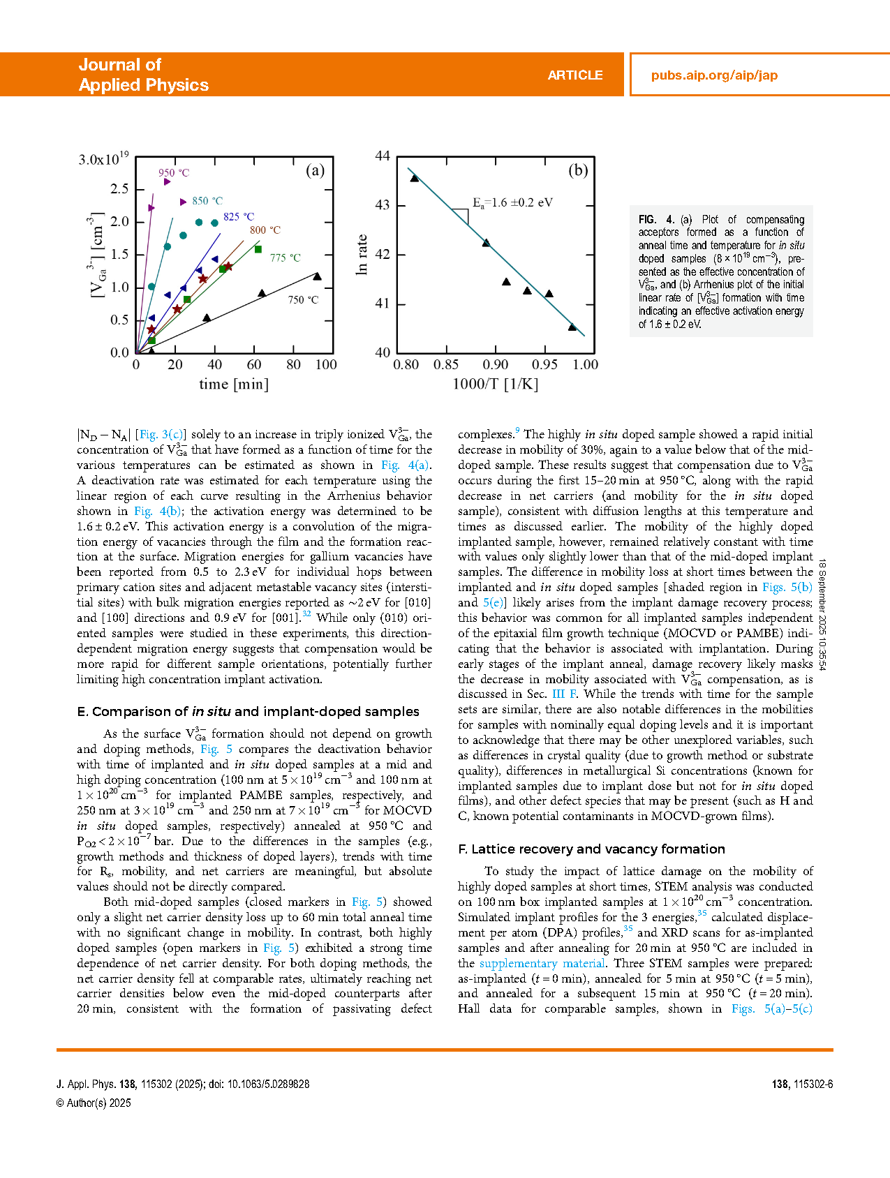
FIG. 4. (a) Plot of compensating acceptors formed as a function of anneal time and temperature for in situ doped samples (8 × 1019 cm−3), presented as the effective concentration of VGa3−, and (b) Arrhenius plot of the initial linear rate of [VGa3−] formation with time indicating an effective activation energy of 1.6 ± 0.2 eV.
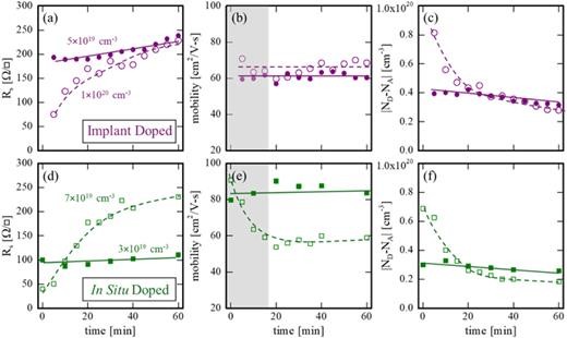
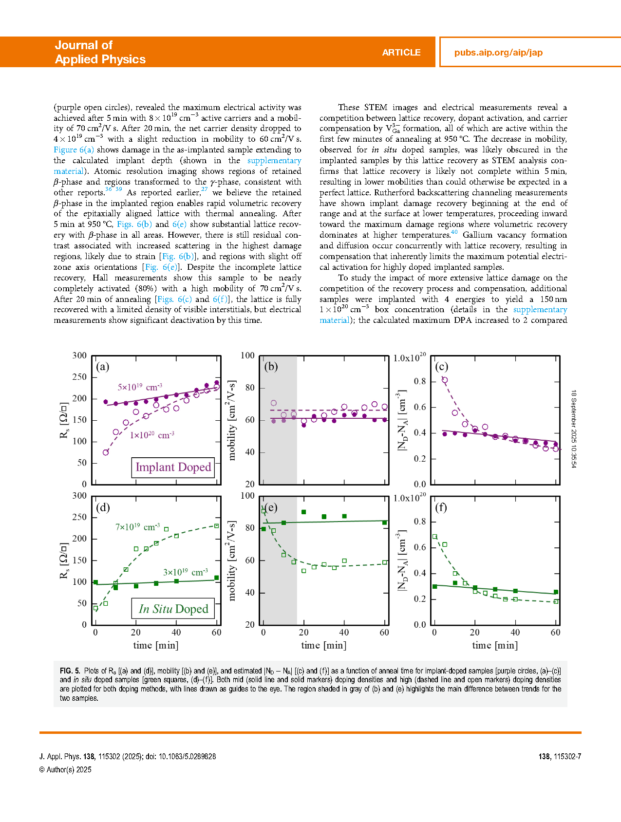
FIG. 5. Plots of Rs [(a) and (d)], mobility [(b) and (e)], and estimated |ND − NA| [(c) and (f)] as a function of anneal time for implant-doped samples [purple circles, (a)–(c)] and in situ doped samples [green squares, (d)–(f)]. Both mid (solid line and solid markers) doping densities and high (dashed line and open markers) doping densities are plotted for both doping methods, with lines drawn as guides to the eye. The region shaded in gray of (b) and (e) highlights the main difference between trends for the two samples.
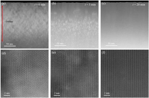
FIG. 6. Cross-sectional STEM images for samples implanted to 1 × 10²⁰ shown as-implanted [(a) and (d)], after annealing for 5 min resulting in optimized electrical activation [(b) and (e)], and after annealing for 20 min [(c) and (f)]. All samples are viewed along the [001] zone axis of β-Ga2O3. Images (a) and (b) show contrast associated with strain in the damaged regions of the implant, with (c) showing complete recovery. Images (d)–(f) are taken from the regions of highest damage.
DOI:
doi.org/10.1063/5.0289828