Paper Sharing
【International Papers】Hydrogen passivation of electron traps and fixed charges in SiO₂/β-Ga₂O₃(001) MOS structures
日期:2025-10-24阅读:507
Researchers from the The University of Osaka have published a dissertation titled "Hydrogen passivation of electron traps and fixed charges in SiO2/β-Ga2O3(001) MOS structures " in Applied Physics Letters.
Background
β-Gallium oxide (β-Ga2O3) has a wide bandgap (4.9 eV) and a high breakdown electric field (8 MV/cm), making it a promising candidate for next-generation power semiconductor materials. The growth processes of β-Ga2O3 bulk crystals, such as the edge-defined film-fed growth method and the Czochralski method, do not require high pressure, resulting in lower manufacturing costs compared with other widegap semiconductors. Single-crystalline β-Ga2O3 epitaxial layers can be grown by hydride vapor phase epitaxy, and the donor concentration can be controlled over a wide range: 1015–1019 cm−3. Despite these advantages, Ga2O3 suffers from low thermal conductivity and challenges in achieving p-type conduction. The former problem can be compensated by placing Ga2O3 on top of high-thermal-conductivity materials such as silicon carbide. As for the latter, a solution is to use a semi-insulating region instead of p-type region in the device structure. A variety of power devices, including vertical Schottky barrier diodes, depletion-mode metal-oxide-semiconductor field-effect transistors (MOSFETs), and superjunction-equivalent MOSFETs, have been reported so far, highlighting the growing interest in Ga2O3.
In the present study, we investigated the impact of post-metallization forming gas annealing (FG-PMA) on the interface and dielectric properties of SiO2/β-Ga2O3 MOS structures. In the case of Si MOS structures, FG annealing is known to introduce hydrogen atoms that efficiently terminate the silicon dangling bonds (Pb center) at the SiO2/Si interface. Hydrogen atoms are also effective in passivating the carbon-dangling bonds (PbC center) at the SiO2/SiC interface. Unlike these covalent semiconductors, Ga2O3 has an ionic bonding character, but it is still meaningful to examine the impact of FG-PMA, which is widely used in semiconductor technology.
Abstract
We investigated the effect of post-metallization forming gas annealing (FG-PMA) on SiO2/β-gallium oxide [β-Ga2O3(001)] MOS structures. We found that FG-PMA at a relatively low temperature (200–400 °C) efficiently reduced the interface and near-interface defects, resulting in improvements to device performance and reliability. By performing FG-PMA after post-deposition annealing in O2 and N2 atmospheres, the interface state density near the conduction band edge of Ga2O3 was reduced to as low as (4–7) × 1010 eV−1 cm−2. The significant improvement in electrical properties was attributed to the passivation of electrical defects by hydrogen atoms.
Conclusion
In summary, the investigation of the effect of FG-PMA on SiO2/β-Ga2O3(001) MOS structures confirmed that FG-PMA at a relatively low temperature (200–400 °C) reduced interface defects, fixed charges, and near-interface oxide traps. By performing FG-PMA after combined O2 and N2 annealing, the interface state density near the conduction band edge of Ga2O3 was reduced to as low as (4–7) × 1010 eV−1 cm−2. These improvements in electrical properties are attributed to passivation of defects by hydrogen atoms.
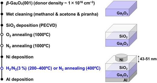
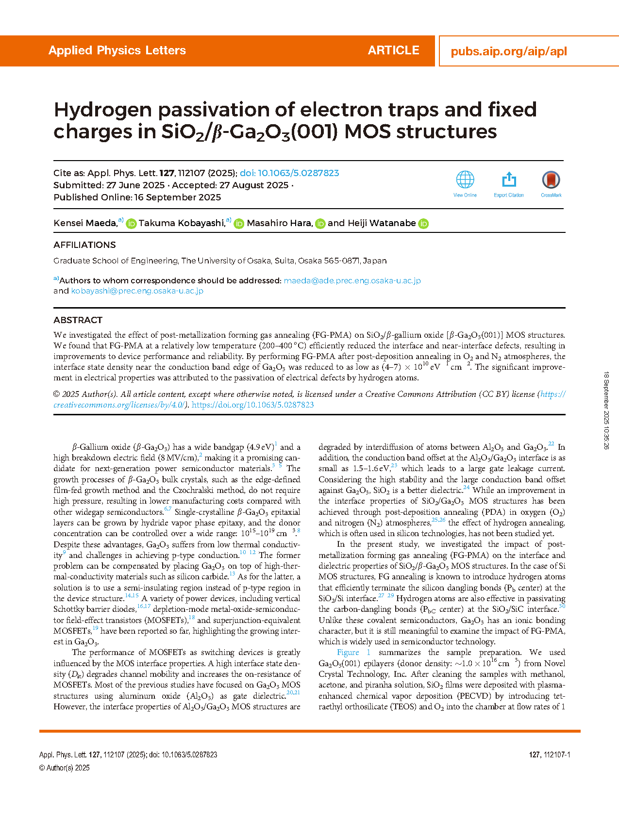
FIG. 1. Flow of fabricating Ga2O3 MOS structures.
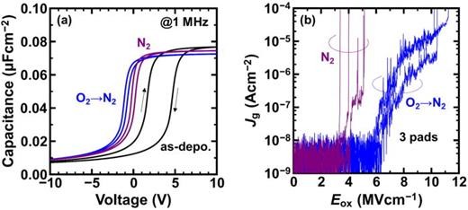
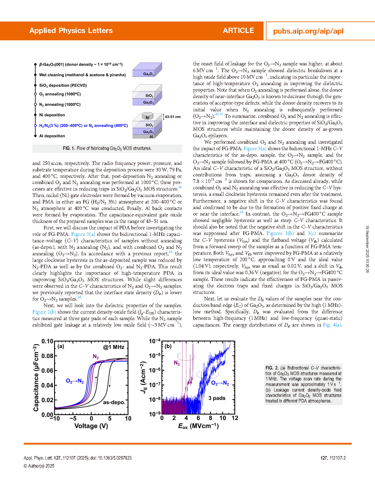
FIG. 2. (a) Bidirectional C–V characteristics of Ga2O3 MOS structures measured at 1 MHz. The voltage scan rate during the measurement was approximately 1 V s−1. (b) Leakage current density-oxide field characteristics of Ga2O3 MOS structures treated in different PDA atmospheres.
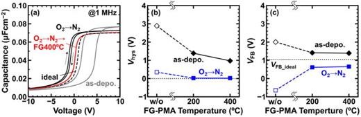
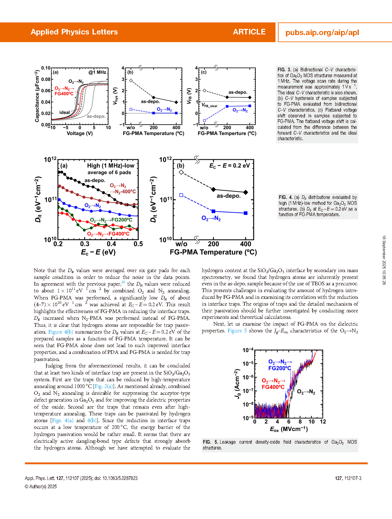
FIG. 3. (a) Bidirectional C–V characteristics of Ga2O3 MOS structures measured at 1 MHz. The voltage scan rate during the measurement was approximately 1 V s−1. The ideal C–V characteristic is also shown. (b) C–V hysteresis of samples subjected to FG-PMA evaluated from bidirectional C–V characteristics. (c) Flatband voltage shift observed in samples subjected to FG-PMA. The flatband voltage shift is calculated from the difference between the forward C–V characteristics and the ideal characteristic.
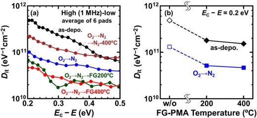
FIG. 4. (a) Dit distributions evaluated by high (1 MHz)-low method for Ga2O3 MOS structures. (b) Dit at EC−E = 0.2 eV as a function of FG-PMA temperature.
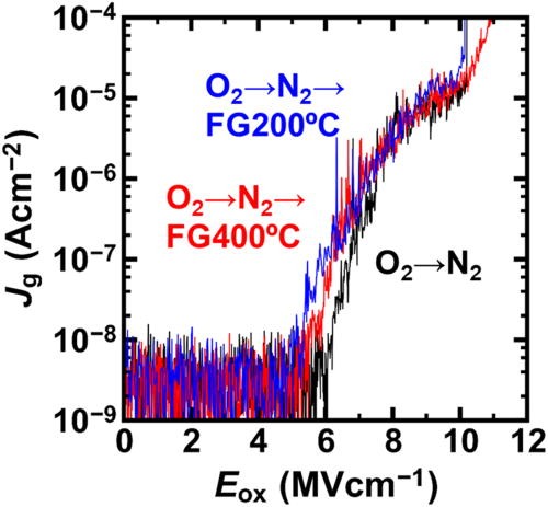
FIG. 5. Leakage current density-oxide field characteristics of Ga2O3 MOS structures.
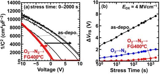
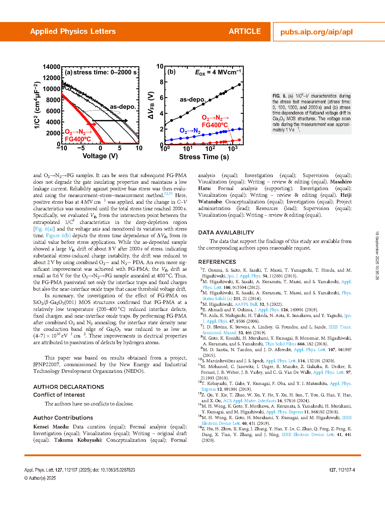
FIG. 6. (a) 1/C2–V characteristics during the stress test measurement (stress time: 0, 100, 1000, and 2000 s) and (b) stress time dependence of flatband voltage drift in Ga2O3 MOS structures. The voltage scan rate during the measurement was approximately 1 V s−1.
DOI:
doi.org/10.1063/5.0287823