Paper Sharing
【International Papers】Quasi-vertical β-Ga₂O₃ Schottky diodes on sapphire using all-LPCVD growth and plasma-free Ga-assisted etching
日期:2025-10-27阅读:561
Researchers from the University of Massachusetts Lowell have published a dissertation titled "Quasi-vertical β-Ga2O3 Schottky diodes on sapphire using all-LPCVD growth and plasma-free Ga-assisted etching" in APL Electronic Devices.
Background
β-Ga2O3 stands out as a promising ultra-wide bandgap semiconductor for next-generation high-voltage, high-efficiency power electronics, due to its ultra-wide bandgap (∼4.8 eV), high breakdown electric field (6–8 MV/cm), and the availability of low-cost, large-area native substrates grown by melt-based growth methods. These characteristics result in Baliga’s figure of merit that surpasses those of conventional wide bandgap power semiconductors such as SiC and GaN, making β-Ga2O3 an ideal candidate for next-generation power conversion systems, radio frequency amplification, and extreme-environment electronics. Substantial progress in high-quality β-Ga2O3 epitaxial film growth has enabled the realization of both lateral and vertical device architectures with excellent breakdown strength and thermal stability. To fully leverage the potential of β-Ga2O3 in high-power vertical device architectures, precise control over vertical isolation and trench formation is essential. This requires fabrication techniques capable of defining deep, high-aspect-ratio structures with minimal damage and high fidelity. However, the absence of p-type doping in β-Ga2O3 necessitates electric field control through mesa, trench, or fin geometries, structures that are highly sensitive to processing-induced surface degradation.
Abstract
This work demonstrates quasi-vertical β-Ga2O3 Schottky barrier diodes (SBDs) fabricated on c-plane sapphire substrates using an all-low-pressure chemical vapor deposition (LPCVD)-based, plasma-free process flow that integrates both epitaxial growth of a high-quality β-Ga2O3 heteroepitaxial film with in situ Ga-assisted β-Ga2O3 etching. A 6.3 μm thick (-201) oriented β-Ga2O3 epitaxial layer structure was grown on c-plane sapphire with 6° miscut, comprising a moderately Si-doped (2.1 × 1017 cm−3) 3.15 μm thick drift layer and a heavily doped (1 × 1019 cm−3) contact layer on an unintentionally doped buffer layer. Mesa isolation was achieved via Ga-assisted plasma-free LPCVD etching, producing ∼60° inclined mesa sidewalls with an etch depth of 3.6 μm. The fabricated SBDs exhibited excellent forward current–voltage characteristics, including a turn-on voltage of 1.22 V, an ideality factor of 1.29, and a Schottky barrier height of 0.83 eV. The minimum differential specific on-resistance was measured to be 8.6 mΩ cm2, and the devices demonstrated high current density capability (252 A/cm2 at 5 V). Capacitance–voltage analysis revealed a net carrier concentration of 2.1 × 1017 cm−3, uniformly distributed across the β-Ga2O3 drift layer. Temperature-dependent J–V–T measurements, conducted from 25 to 250 °C, revealed thermionic emission-dominated transport with strong thermal stability. The Schottky barrier height increased from 0.80 to 1.16 eV, and the ideality factor rose modestly from 1.31 to 1.42 over this temperature range. Reverse leakage current remained low, increasing from ∼5 × 10⁻⁶ A/cm2 at 25 °C to ∼1 × 10⁻⁴ A/cm2 at 250 °C, with the Ion/Ioff ratio decreasing from ∼1 × 10⁷ to 5 × 10⁵. The devices achieved breakdown voltages ranging from 73 to 100 V, corresponding to parallel-plate electric field strengths of 1.66–1.94 MV/cm. These results highlight the potential of LPCVD-grown and etched β-Ga2O3 devices for high-performance, thermally resilient power electronics applications.
Conclusion
In summary, this work demonstrates the first realization of quasi-vertical β-Ga2O3 Schottky barrier diodes fabricated entirely using a plasma-free LPCVD-based process, from epitaxial growth to in situ etching for mesa isolation, on insulating sapphire substrates. Leveraging the in situ Ga-assisted LPCVD etching technique, we achieved plasma damage-free mesa isolation with an etch depth of 3.6 μm and ∼60° inclined sidewalls. The resulting SBDs exhibited excellent forward characteristics with an ideality factor of 1.29, a Schottky barrier height of 0.83 eV, and a low specific on-resistance of 8.6 mΩ cm2. Temperature-dependent I–V–T analysis revealed thermionic emission-dominated transport with strong thermal stability and a modest increase in Schottky barrier height and ideality factor, likely attributed to interface inhomogeneities and barrier non-uniformity. The devices exhibited low and stable reverse leakage characteristics, achieving breakdown fields of up to 1.94 MV/cm. Although the breakdown voltage was limited by the relatively high drift layer doping concentration, the demonstrated reverse blocking capability, along with robust forward conduction and thermal performance, highlight the promise of LPCVD-grown and etched β-Ga2O3 devices. The integration of epitaxy and etching within a single LPCVD platform offers a scalable and low-damage fabrication route for next-generation UWBG power electronics. These results also provide a critical step toward enabling cost-effective, high-voltage, and thermally resilient β-Ga2O3-based device architectures on foreign substrates.
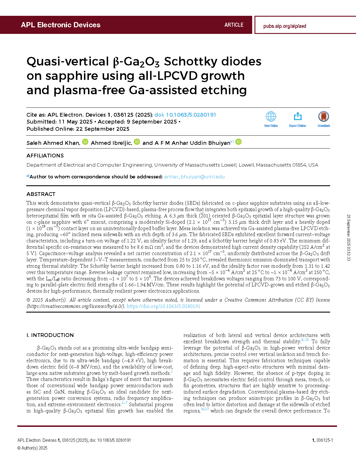
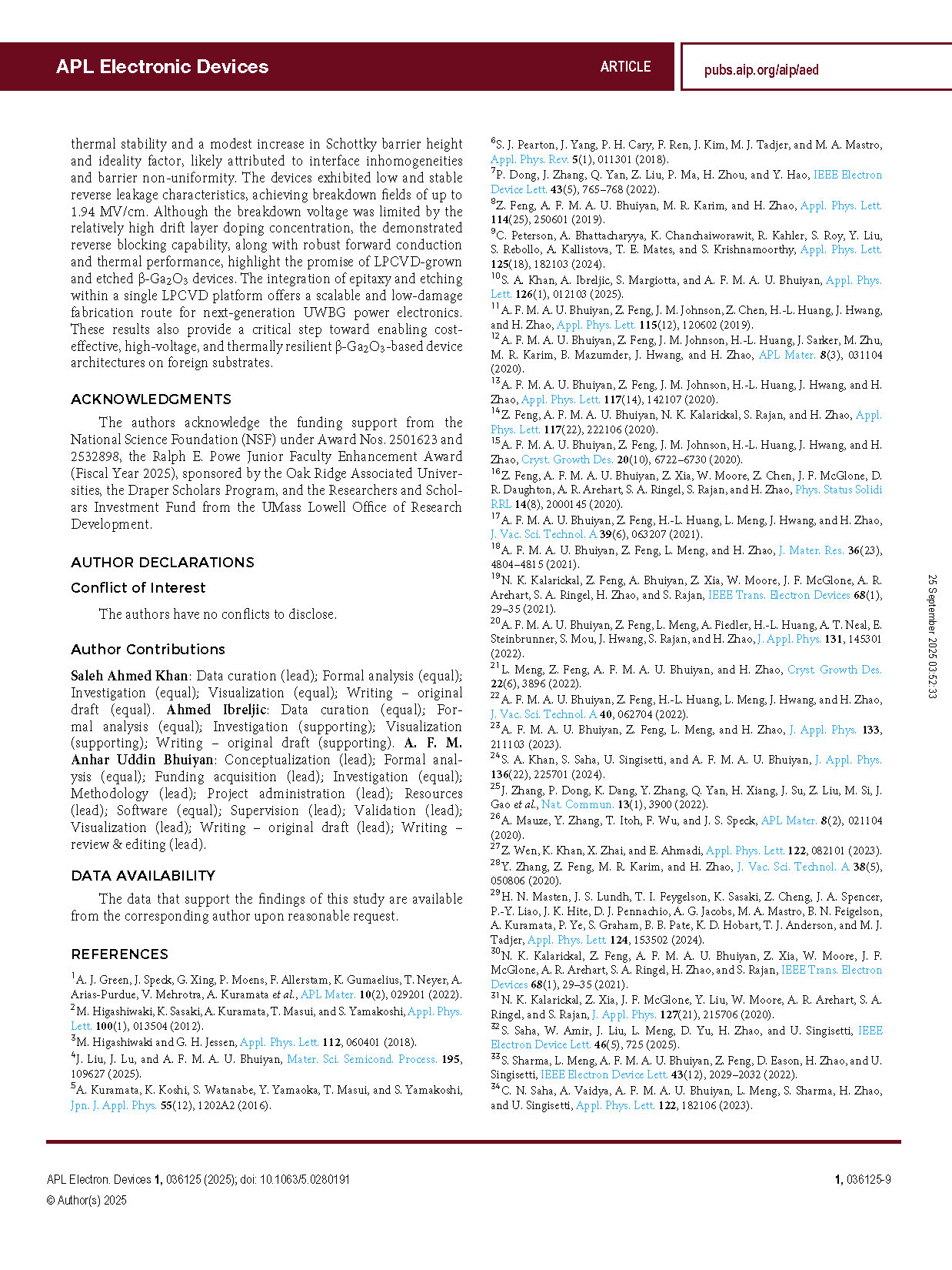
FIG. 1. (a) Schematic cross section of the quasi-vertical Schottky barrier diode (SBD) fabricated using a LPCVD grown (-201) β-Ga2O3 film on a 6° miscut c-plane sapphire substrate. The device features a three-layer epitaxial stack: a 1.05 μm unintentionally doped (UID) buffer layer, a 2.10 μm thick n+ β-Ga2O3 contact layer (Nd = 1 × 1019 cm−3), and a 3.15 μm β-Ga2O3 drift layer (Nd = 2.1 × 1017 cm−3). Plasma-free LPCVD etching was used to etch 3.6 μm into the β-Ga2O3 drift layer for mesa isolation and to expose the n+ layer for anode contact formation. (b) Tilted (60° tilt) cross-sectional FESEM image showing the etch sidewall profile with an etch depth of 3.6 μm. (c) AFM line scan along the AA′ cutline over the etched mesa region, confirming the ∼60° sidewall inclination and an etch depth of 3.6 μm. (d) Step-by-step fabrication process flow including LPCVD growth, in situ etching, and metallization steps for device realization.
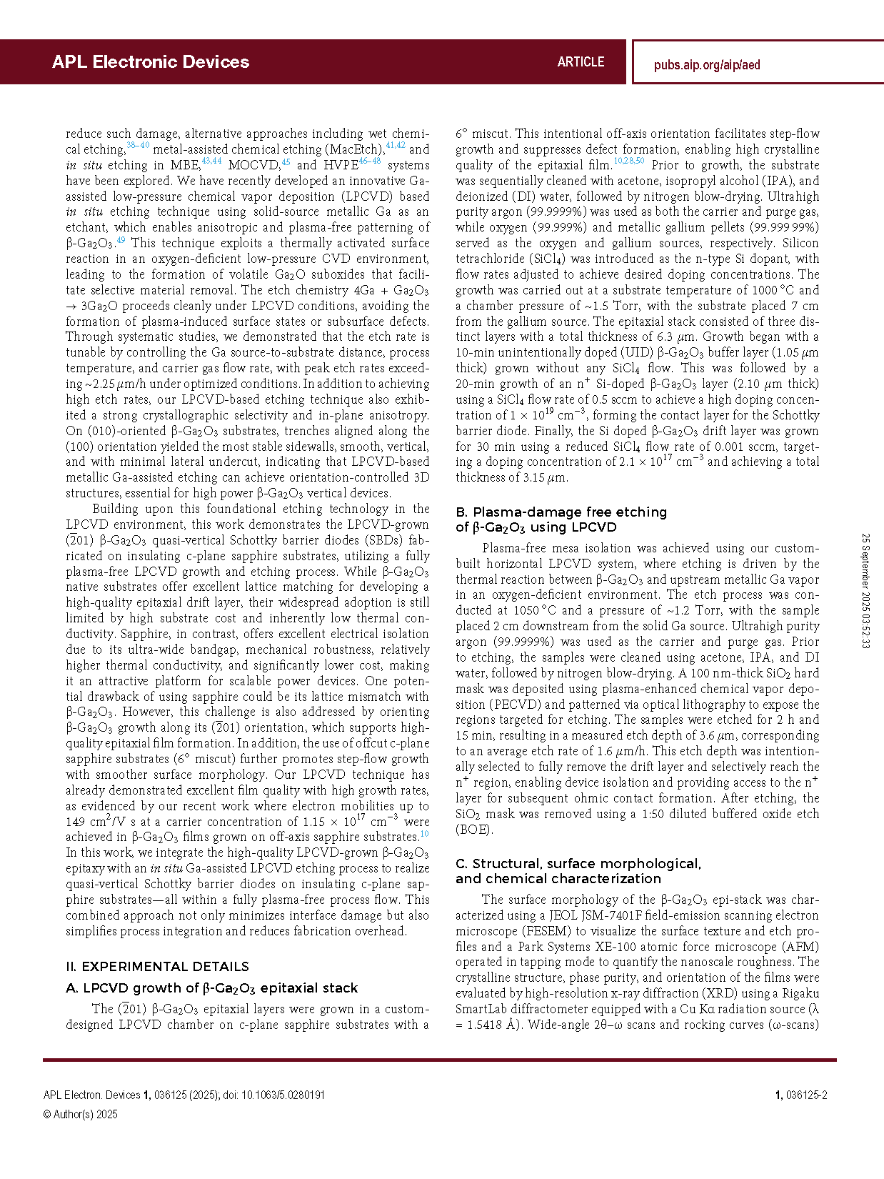
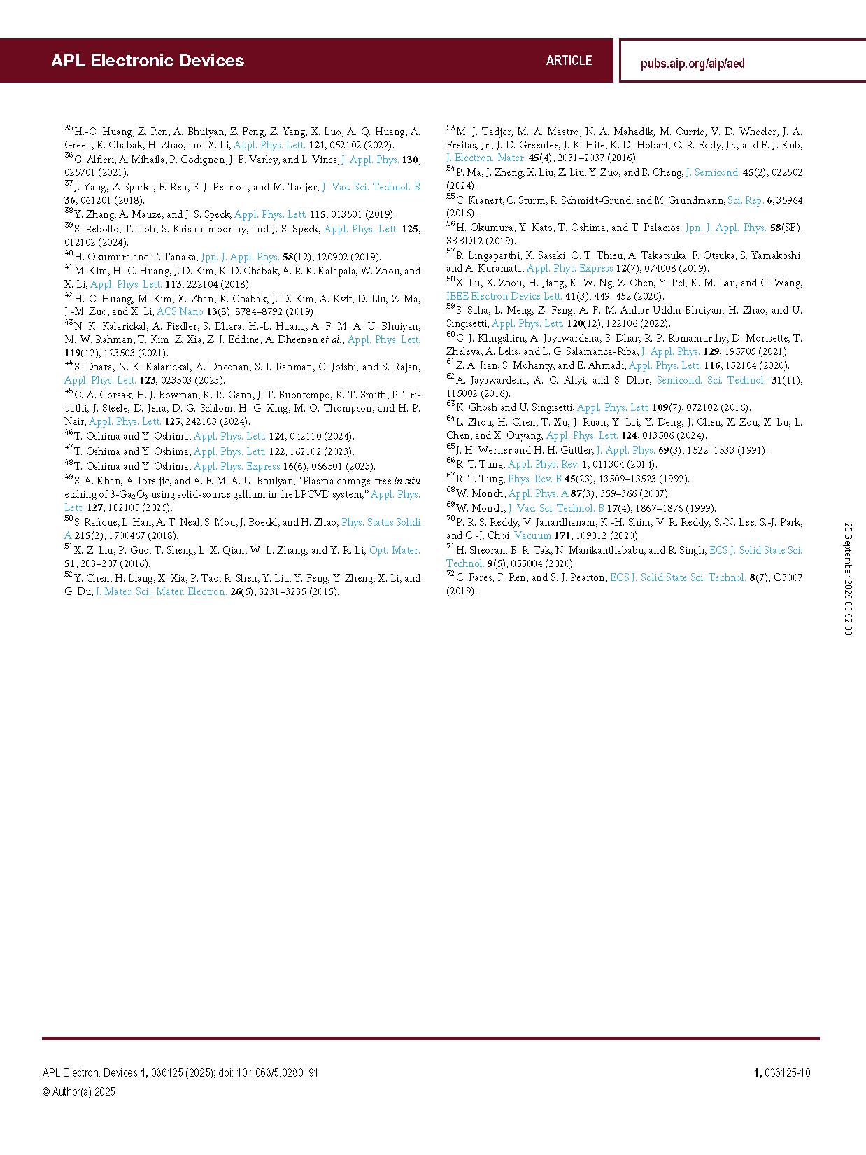
FIG. 2. Structural and surface morphological characterization of the LPCVD-grown heteroepitaxial (-201) β-Ga2O3 epitaxial stack used in device fabrication. (a) Top-view FESEM image showing clear step-flow surface morphology, indicative of high crystalline quality and epitaxial layer-by-layer growth. (b) AFM scan of the film surface reveals smooth morphology with a root mean square (RMS) roughness of 4.7 nm. (c) XRD ω–2θ scan showing strong diffraction peaks corresponding to the (-h0l) family of (-201) β-Ga2O3, along with sapphire substrate peaks, confirming phase purity and preferred orientation. (d) XRD ω-rocking curve of the (-402) reflection exhibiting a narrow full width at half maximum (FWHM) of 287 arcsec, indicating the high crystalline quality of the β-Ga2O3 epitaxial stack.
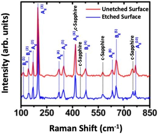
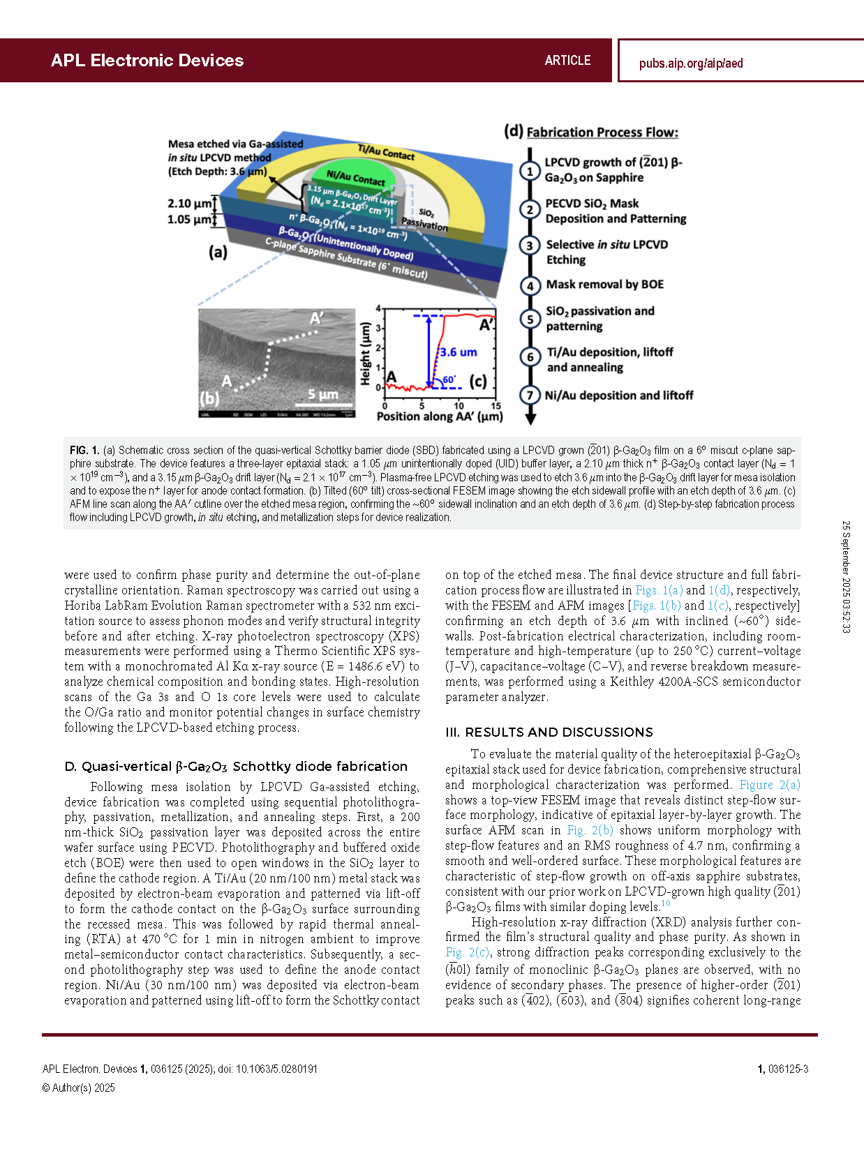
FIG. 3. Room temperature Raman spectra of the LPCVD-grown heteroepitaxial (01) β-Ga2O3 surface before (red) and after (blue) Ga-assisted in situ LPCVD etching. Both spectra exhibit sharp and well-defined Ag and Bg phonon modes characteristic of monoclinic β-Ga2O3, confirming structural integrity and phase purity. Peaks from the c-plane sapphire substrate are also visible in both spectra.
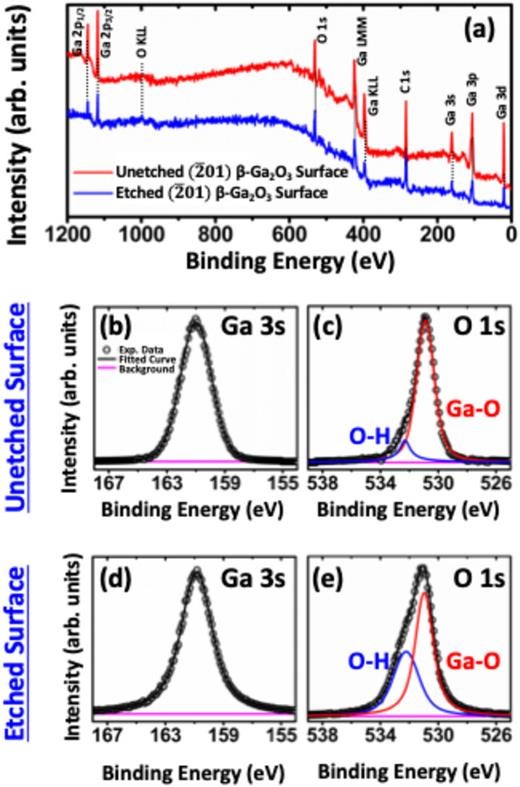
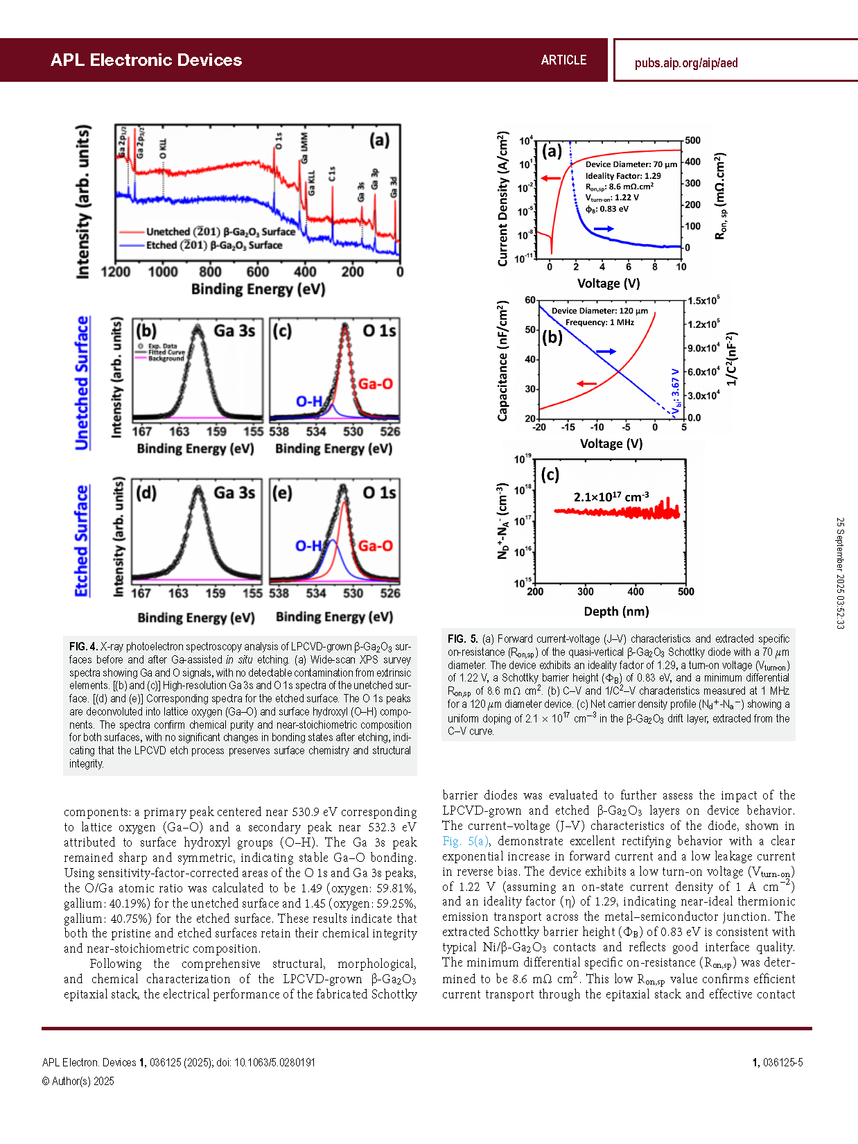
FIG. 4. X-ray photoelectron spectroscopy analysis of LPCVD-grown β-Ga2O3 surfaces before and after Ga-assisted in situ etching. (a) Wide-scan XPS survey spectra showing Ga and O signals, with no detectable contamination from extrinsic elements. [(b) and (c)] High-resolution Ga 3s and O 1s spectra of the unetched surface. [(d) and (e)] Corresponding spectra for the etched surface. The O 1s peaks are deconvoluted into lattice oxygen (Ga–O) and surface hydroxyl (O–H) components. The spectra confirm chemical purity and near-stoichiometric composition for both surfaces, with no significant changes in bonding states after etching, indicating that the LPCVD etch process preserves surface chemistry and structural integrity.
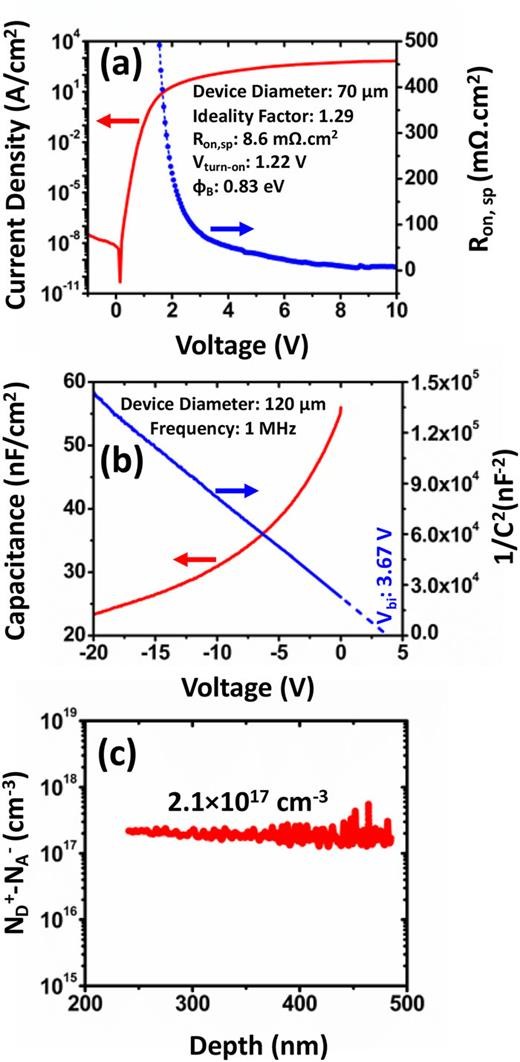
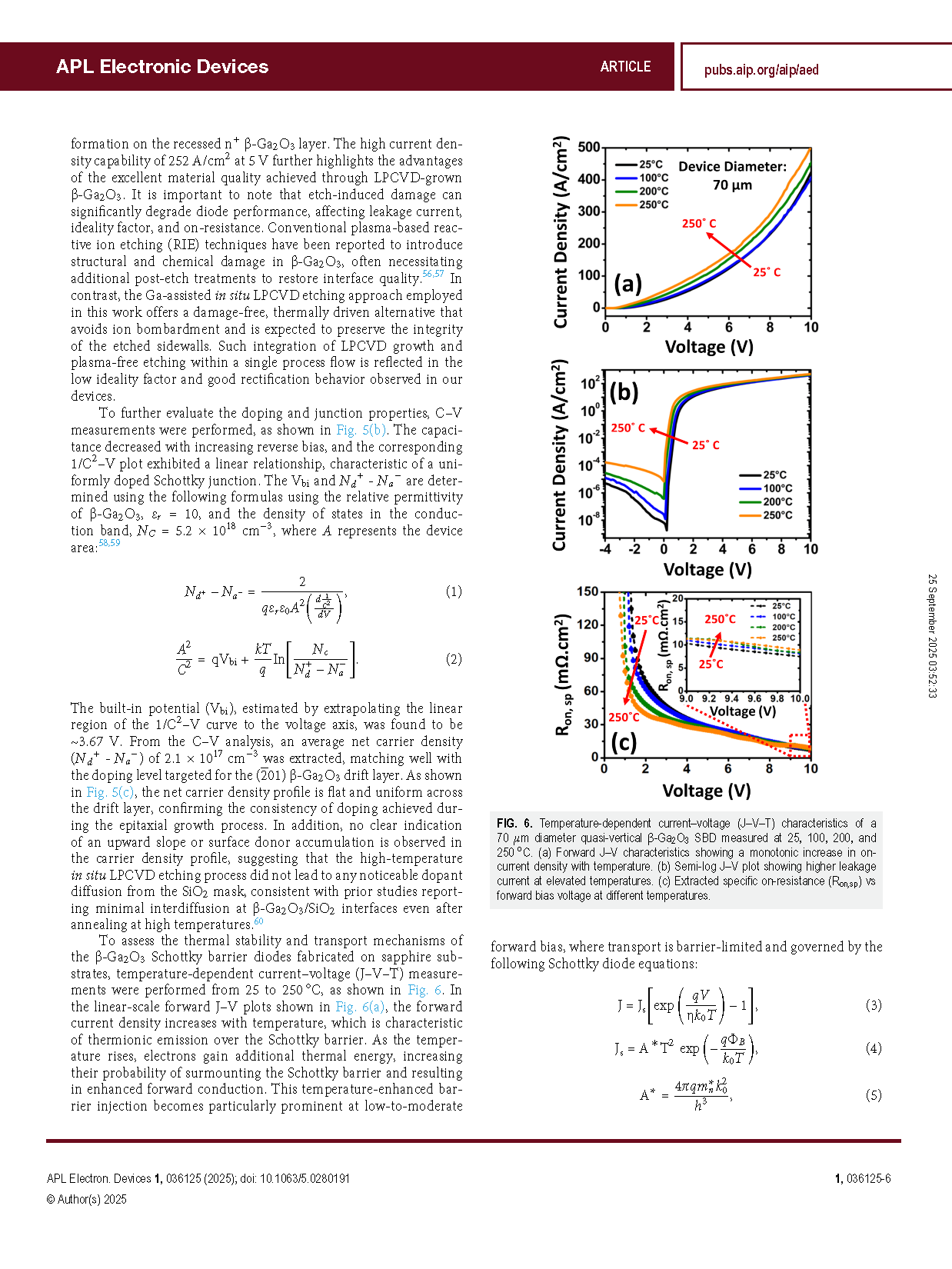
FIG. 5. (a) Forward current-voltage (J–V) characteristics and extracted specific on-resistance (Ron,sp) of the quasi-vertical β-Ga2O3 Schottky diode with a 70 μm diameter. The device exhibits an ideality factor of 1.29, a turn-on voltage (Vturn-on) of 1.22 V, a Schottky barrier height (ΦB) of 0.83 eV, and a minimum differential Ron,sp of 8.6 mΩ cm2. (b) C–V and 1/C2–V characteristics measured at 1 MHz for a 120 μm diameter device. (c) Net carrier density profile (Nd+-Na−) showing a uniform doping of 2.1 × 1017 cm−3 in the β-Ga2O3 drift layer, extracted from the C–V curve.
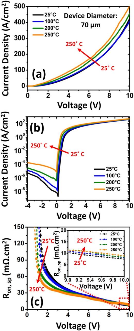
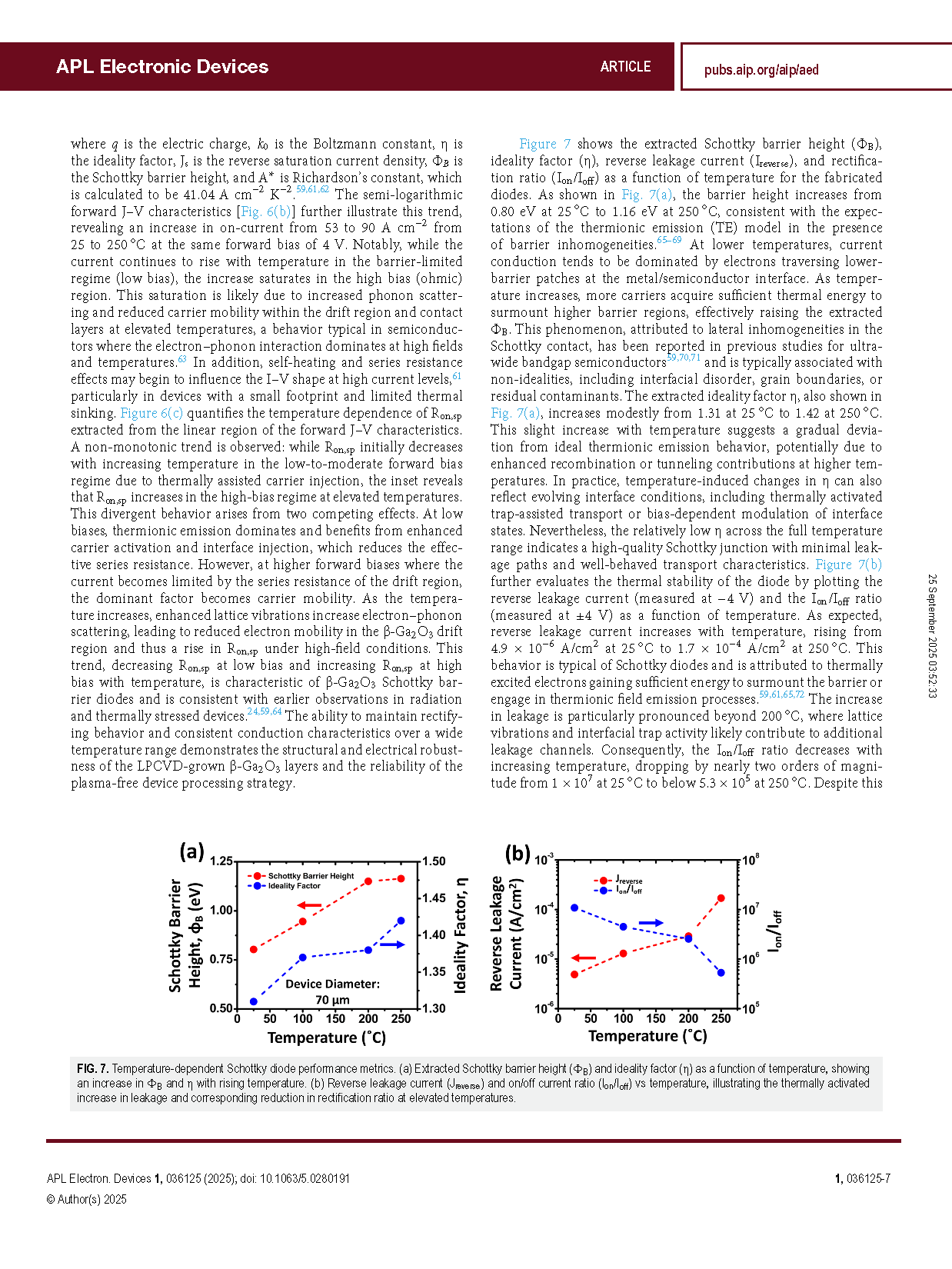
FIG. 6. Temperature-dependent current–voltage (J–V–T) characteristics of a 70 μm diameter quasi-vertical β-Ga2O3 SBD measured at 25, 100, 200, and 250 °C. (a) Forward J–V characteristics showing a monotonic increase in on-current density with temperature. (b) Semi-log J–V plot showing higher leakage current at elevated temperatures. (c) Extracted specific on-resistance (Ron,sp) vs forward bias voltage at different temperatures.
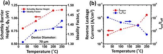
FIG. 7. Temperature-dependent Schottky diode performance metrics. (a) Extracted Schottky barrier height (ΦB) and ideality factor (η) as a function of temperature, showing an increase in ΦB and η with rising temperature. (b) Reverse leakage current (Jreverse) and on/off current ratio (Ion/Ioff) vs temperature, illustrating the thermally activated increase in leakage and corresponding reduction in rectification ratio at elevated temperatures.
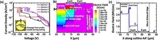
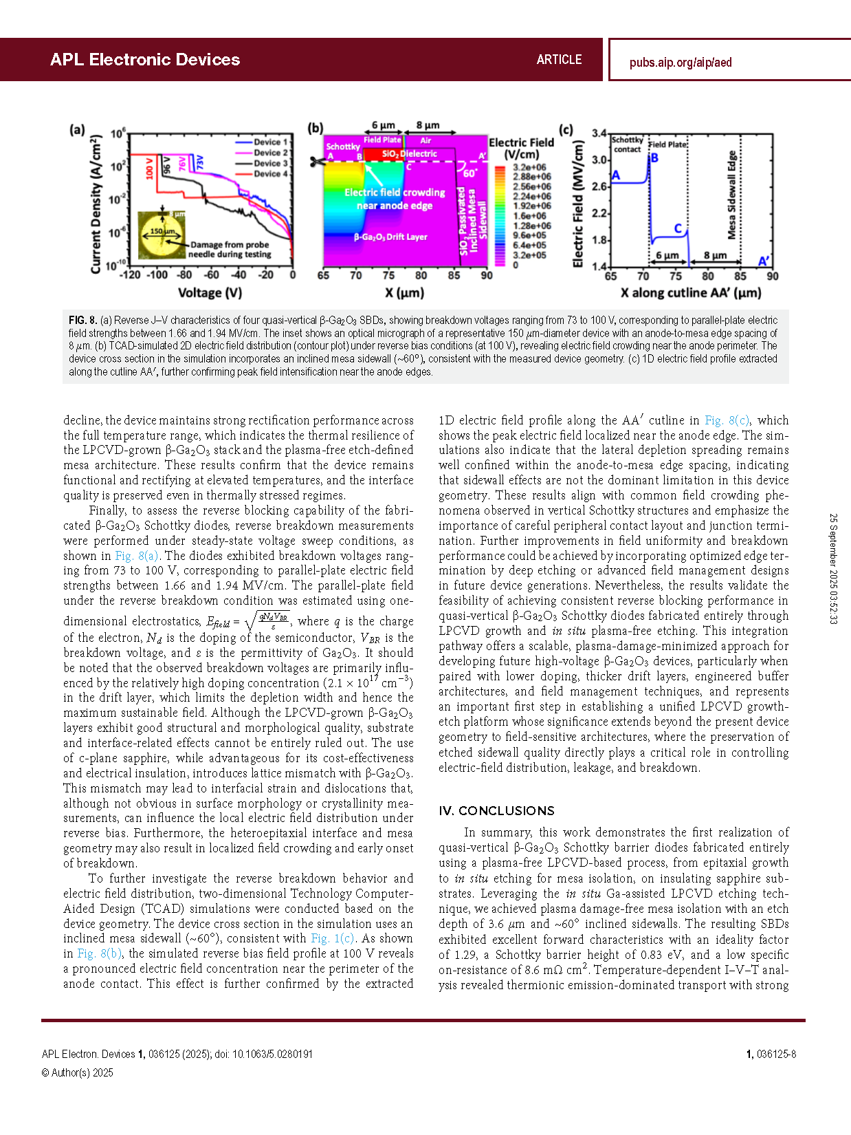
FIG. 8. (a) Reverse J–V characteristics of four quasi-vertical β-Ga2O3 SBDs, showing breakdown voltages ranging from 73 to 100 V, corresponding to parallel-plate electric field strengths between 1.66 and 1.94 MV/cm. The inset shows an optical micrograph of a representative 150 μm-diameter device with an anode-to-mesa edge spacing of 8 μm. (b) TCAD-simulated 2D electric field distribution (contour plot) under reverse bias conditions (at 100 V), revealing electric field crowding near the anode perimeter. The device cross section in the simulation incorporates an inclined mesa sidewall (∼60°), consistent with the measured device geometry. (c) 1D electric field profile extracted along the cutline AA′, further confirming peak field intensification near the anode edges.
DOI:
doi.org/10.1063/5.0280191