Paper Sharing
【International Papers】Status of Ga₂O₃ for power device and UV photodetector applications
日期:2025-10-28阅读:609
Researchers from the University of Florida have published a dissertation titled "Status of Ga2O3 for power device and UV photodetector applications" in Applied Physics Reviews.
Background
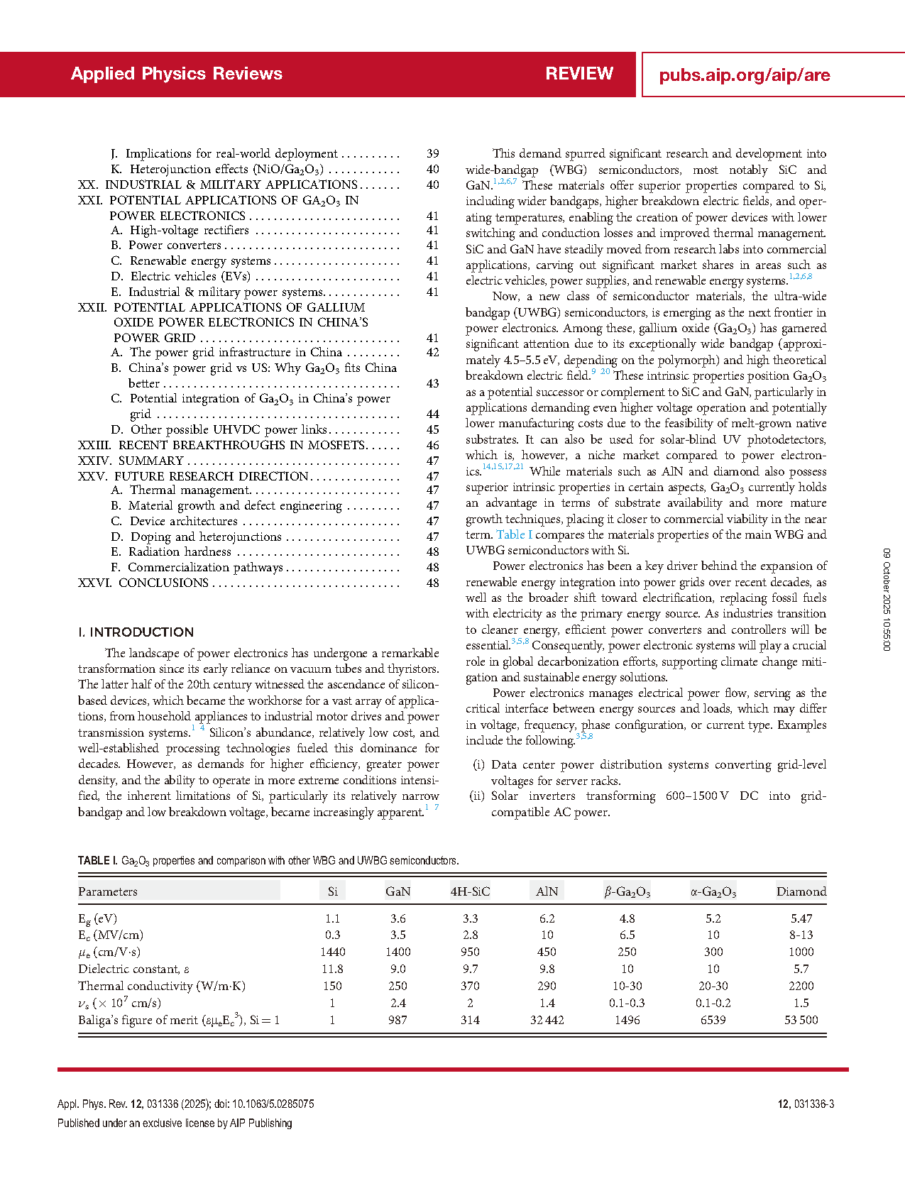
The landscape of power electronics has undergone a remarkable transformation since its early reliance on vacuum tubes and thyristors. The latter half of the 20th century witnessed the ascendance of silicon-based devices, which became the workhorse for a vast array of applications, from household appliances to industrial motor drives and power transmission systems. Silicon’s abundance, relatively low cost, and well-established processing technologies fueled this dominance for decades. However, as demands for higher efficiency, greater power density, and the ability to operate in more extreme conditions intensified, the inherent limitations of Si, particularly its relatively narrow bandgap and low breakdown voltage, became increasingly apparent.
Abstract
Gallium oxide (Ga2O3) has been the subject of extensive research over the past decade due to its potential in next-generation power electronics and solar-blind ultraviolet (UV) photodetectors. While Ga2O3 exhibits promising material characteristics for applications in harsh environments, its commercial viability remains under debate, particularly when compared to materials such as aluminum nitride (AlN) and diamond, which possess superior intrinsic properties. This perspective addresses the critical challenges that currently impede the widespread commercialization of Ga2O3-based devices. These challenges include a relatively immature technology base, the difficulty in achieving stable p-type conductivity, inherently low thermal conductivity, the presence of crystallographic defects (nano- and micro-voids), and elevated fabrication costs, all of which negatively impact device reliability and scalability. Mitigation strategies, such as heterojunction implementation, the development of thermal management solutions such as wafer bonding, and defect passivation approaches, are also under investigation. The near-term feasibility of commercially viable Ga2O3-based power electronic devices is a central focus of this discussion. The current status is that Ga2O3 development is far advanced relative to either diamond or especially AlN power electronics but is hampered by lack of a broad base of substrate vendors and a compelling vision for device implementations that provide sufficient improvement over SiC power devices. There are strong geographic differences in device focus, with China prioritizing implementation in grid applications while the United States/Europe appear to consider Ga2O3 devices more for defense and aerospace applications.
Conclusion
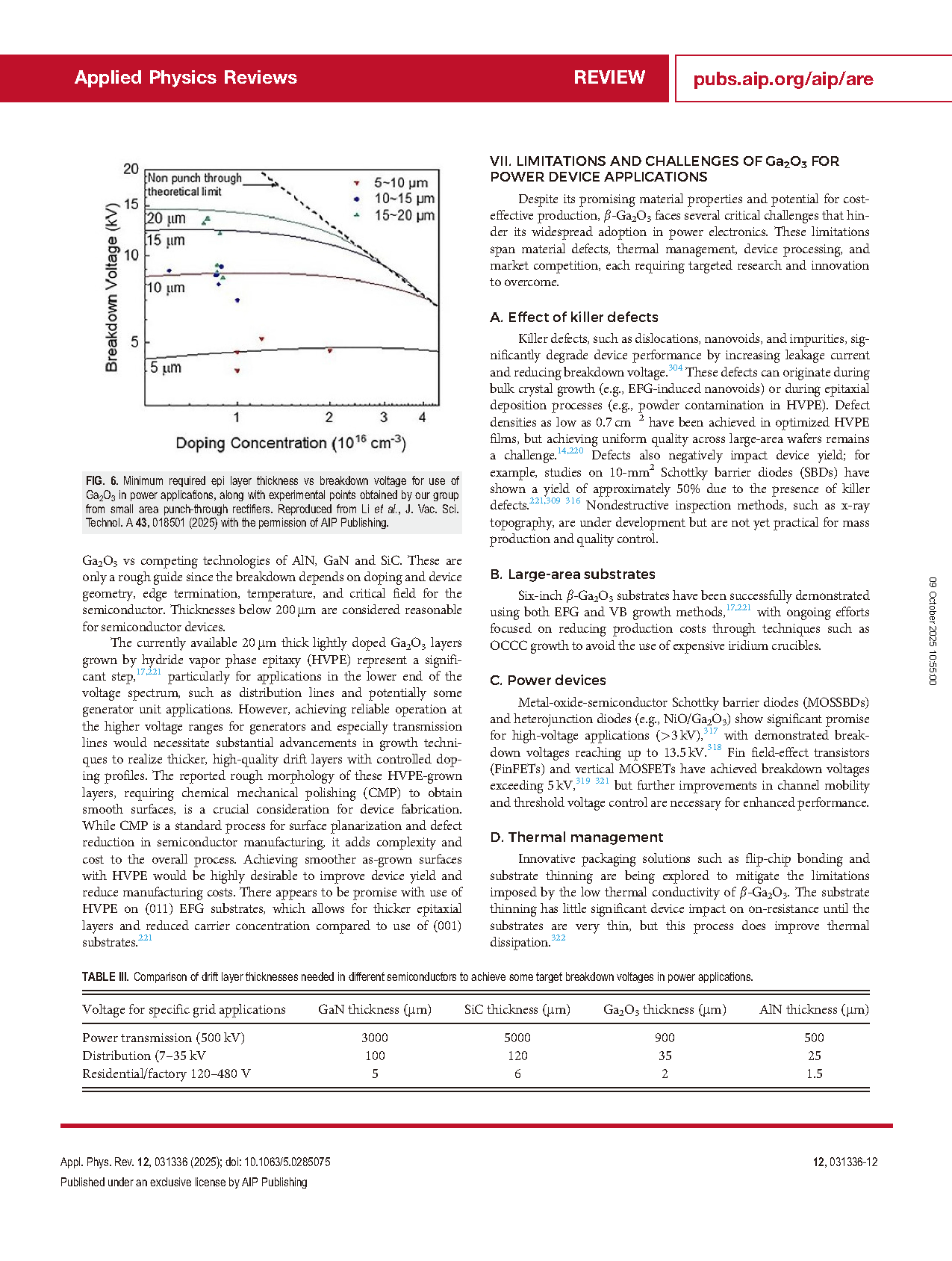
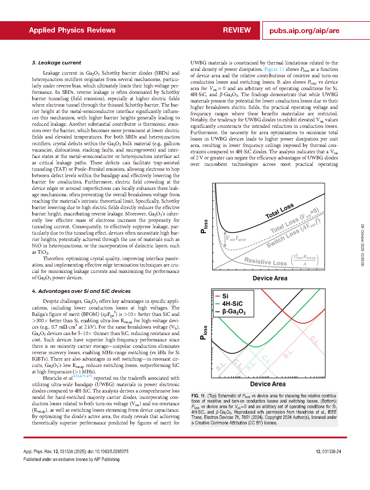
Ga2O3 holds promise for next-generation power electronics, offering higher efficiency, power density, and temperature resilience in power electronics than silicon. However, achieving commercial viability requires breakthroughs in material growth, device fabrication, and system integration. As electrification accelerates, Ga2O3 could play a pivotal role in building a sustainable energy future, provided these challenges are addressed. The market for solar-blind UV photodetection is much smaller, and it is not clear that Ga2O3 has advantages over competing technologies. China and the United States are both investing in Ga2O3 for power electronics, but with likely different focuses. China has more use for ultrahigh-voltage (UHV) grid applications, while the United States is likely to focus on defense, aerospace, and medium-voltage industrial uses. For China, a priority would be to accelerate Ga2O3 diode deployment in UHV substations. The R&D Focus in that case is to improve thermal packaging for grid-scale reliability. For the United States, the priority would be to leverage Ga2O3 in defense systems and monitor grid potential. In that case, the R&D Focus might be hybrid Ga2O3-SiC modules for industrial power systems. Ga2O3 is clearly not a replacement for SiC/GaN but could revolutionize ultrahigh-voltage power grids. The U.S. and Europe may follow in defense and transport applications, but widespread grid adoption depends on solving thermal and reliability hurdles. It is important to note the projections for grid expansion due to projected AI implementation. To meet the projected explosive growth of AI, power grids in the United States and China must undergo unprecedented expansion. The energy demands of AI data centers highlight the need for infrastructure upgrades. both the United States and China must rapidly scale their grids through new renewable energy projects, advanced nuclear power, and grid modernization to avoid bottlenecks. Without such investments, AI’s expansion could outpace the energy supply.
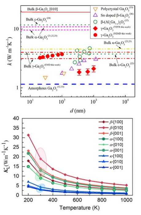
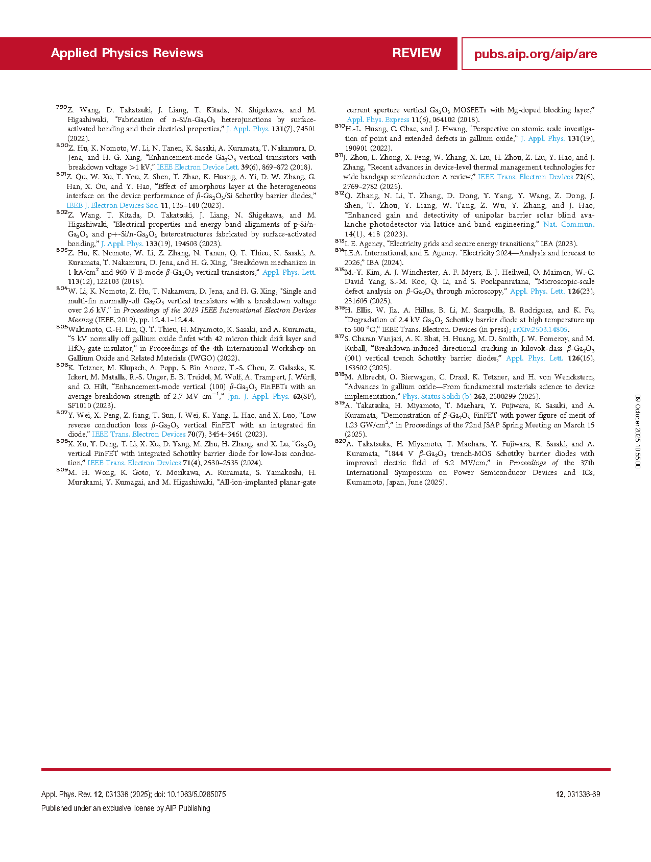
FIG. 1. Summary of the reported values of thermal conductivity of various types of Ga2O3.
FIG. 2. Summary of PL spectra and determination of optical bandgap for different polymorphs of Ga2O3.
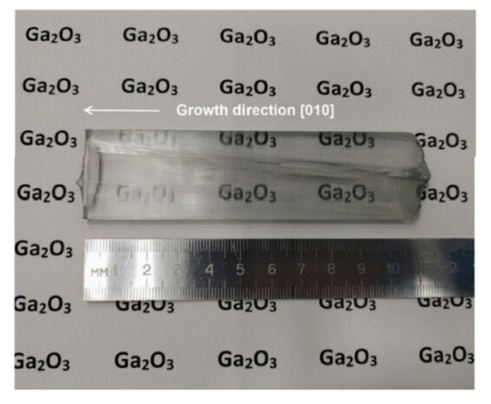
FIG. 3. Photograph of β-Ga2O3 crystals with typical dimensions of 110 mm length and 30 mm width grown by the EFG method.
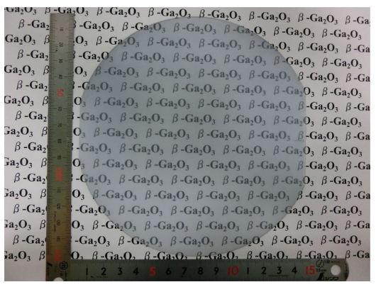
FIG. 4. Picture of 6-inch β-Ga2O3 single crystal substrate.
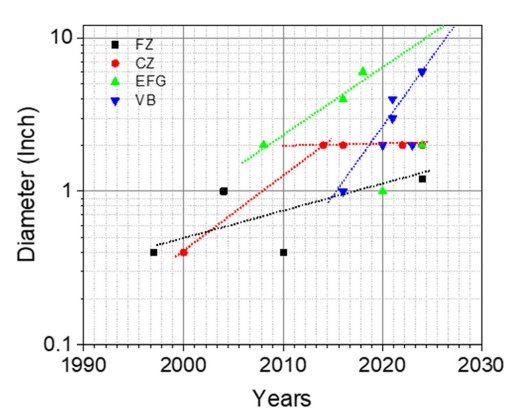
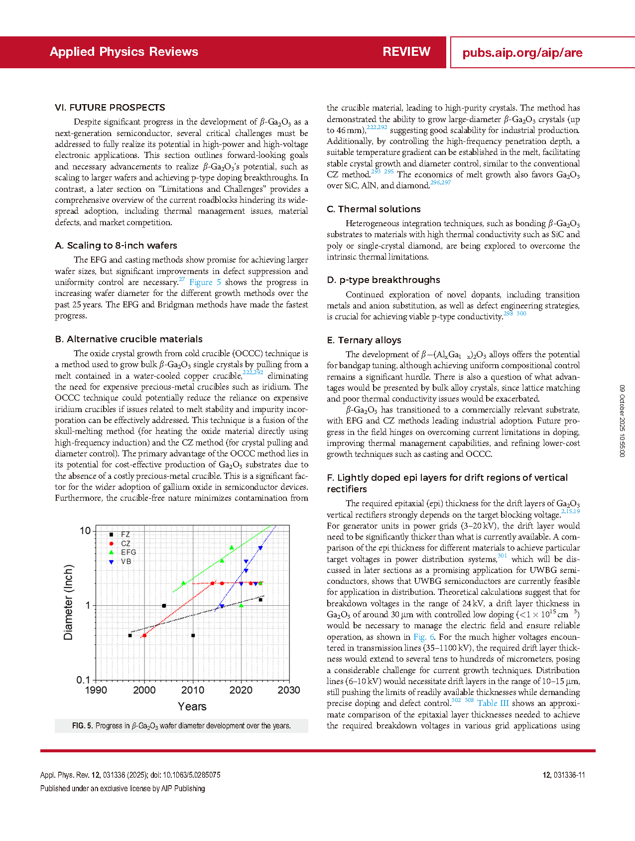
FIG. 5. Progress in β-Ga2O3 wafer diameter development over the years.
DOI:
doi.org/10.1063/5.0285075