Paper Sharing
【Member Papers】Electrical conductance at Ga₂O₃/Si interfaces fabricated via surface activated bonding
日期:2025-10-28阅读:537
Researchers from the National Institute of Advanced Industrial Science and Technology and Novel Crystal Technology, Inc., have published a dissertation titled "Electrical conductance at Ga2O3/Si interfaces fabricated via surface activated bonding" in Journal of Applied Physics.
Background
Beta-phase gallium oxide (β-Ga2O3) exhibits excellent electrical properties, which include a large bandgap, high critical electric field strength, and high saturation electron velocity. These properties have facilitated the development of high-power electronics with low resistance. Furthermore, unlike other wide-gap materials such as SiC, GaN, and diamond, large-sized and high-quality crystals can be synthesized using melt-grown methods, which contributes to the low-cost manufacturing of β-Ga2O3 wafers. Therefore, many researchers consider low-cost β-Ga2O3 wafers suitable candidates for developing low-loss power electronics in the future. However, p-type doping is theoretically challenging, which limits its use in unipolar devices.
Abstract
Under ultrahigh vacuum conditions, β-Ga2O3 and Si surfaces form atomic bonds after surface sputtering treatment. It enables the formation of a β-Ga2O3/Si heterostructure, which can contribute to future high-power devices integrated with conventional systems. However, the surface sputtering step generates crystalline damage, hindering electrical conductance across materials. In this study, sputtering conditions were optimized to maximize electrical conductance, and the effects of annealing were investigated to initiate recrystallization. The current between substrates was maximized when Si was sputtered for 40 s and β-Ga2O3 was not sputtered. In addition, annealing at 500 °C achieved ohmic-like current–voltage characteristics between n-type β-Ga2O3 and n-type Si substrates because of recrystallization. An electrically conductive interface can contribute to heterodevices combining β-Ga2O3 devices, which have difficulty in p-type doping, with other materials.
Conclusion
The effect of Ar fast atom beam irradiation and post-bonding annealing on the electrical conductance of n-type β-Ga2O3 and Si substrates was investigated in this study. The results confirm that the short sputtering of the β-Ga2O3 surface significantly degrades electrical conductance caused by damage at the bonding interface. In addition, the Si surface was sputtered for 40 s to effectively remove the native oxide layer while minimizing crystalline damage. A strong bonding equivalent to the Si bulk is achieved when the Si surface is sputtered and the β-Ga2O3 surface is not. Furthermore, under this bonding condition, annealing over 500 °C can enable ohmic-like contact by recovering the crystalline damage. These findings suggest that careful control of surface activation and annealing processes is important for electrical conductance β-Ga2O3/Si heterostructures, and it can contribute to the development of β-Ga2O3-based heterodevices.
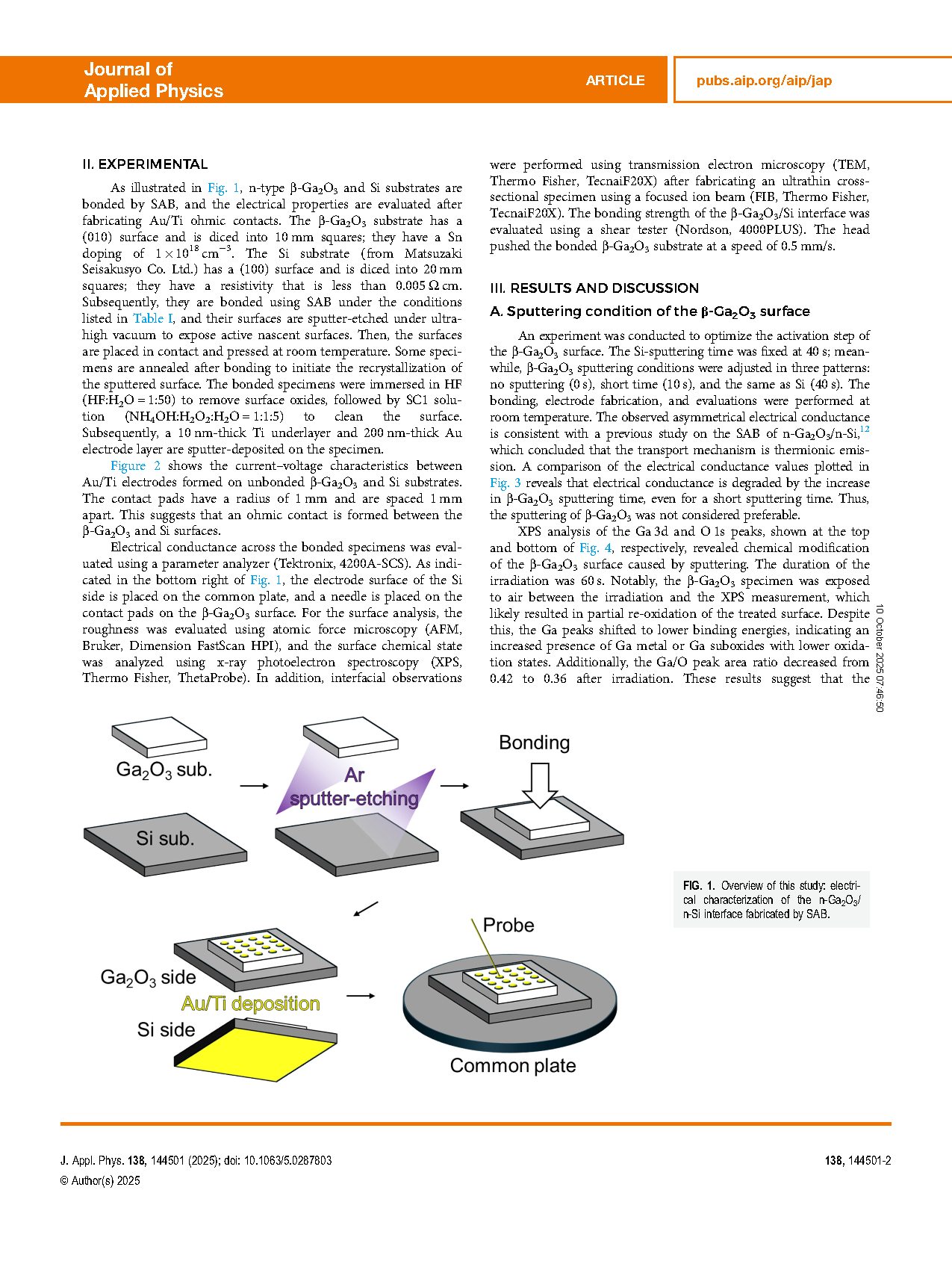
FIG. 1. Overview of this study: electrical characterization of the n-Ga2O3/n-Si interface fabricated by SAB.
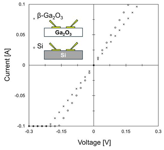
FIG. 2. Current–voltage (I–V) characteristics of Au/Ti contact pads formed on β-Ga2O3 (cross) and Si (circle) surfaces to ensure ohmic contact.
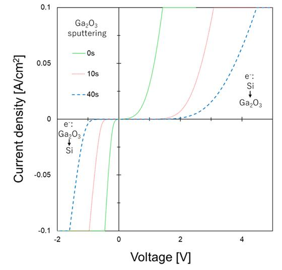
FIG. 3. I–V characteristics of bonded β-Ga2O3/Si specimens under three different sputtering conditions for β-Ga2O3. Electrons moved from Si to β-Ga2O3 at the first quadrant and from β-Ga2O3 to Si at the third quadrant.
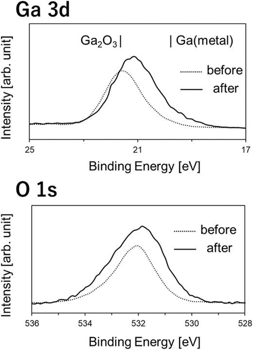
FIG. 4. XPS spectra of Ga 3d and O 1s for the β-Ga2O3 surface before and after 60 s of sputtering. Shift in the Ga 3d peak and variation in the Ga/O peak area ratio suggest chemical modification toward a Ga-rich surface.
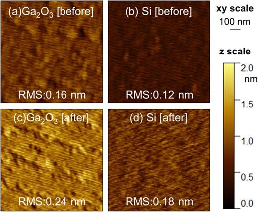
FIG. 5. AFM images of β-Ga2O3 and Si surfaces (a) and (b) before and (c) and (d) after sputtering the Si surface for 40 s. Both surfaces were atomically smooth after sputtering.
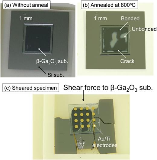
FIG. 6. β-Ga2O3/Si substrates after (a) bonding at room temperature and (b) annealing at 800 °C, which results in unbonded area and cracks. (c) In the shear test, fracture occurred within the Si substrate instead of the bonding interface.
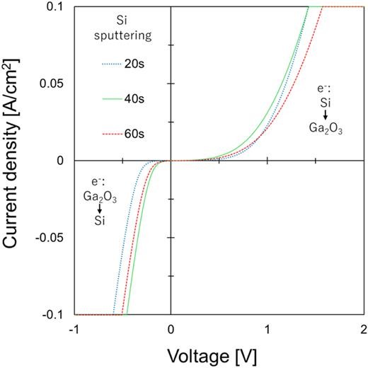
FIG. 7. I–V characteristics of bonded β-Ga2O3/Si specimens under three different sputtering conditions for Si. Sputtering for 40 s is desirable for electrical conductance.
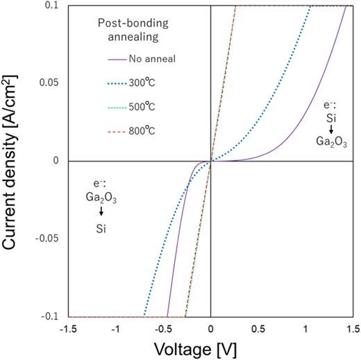
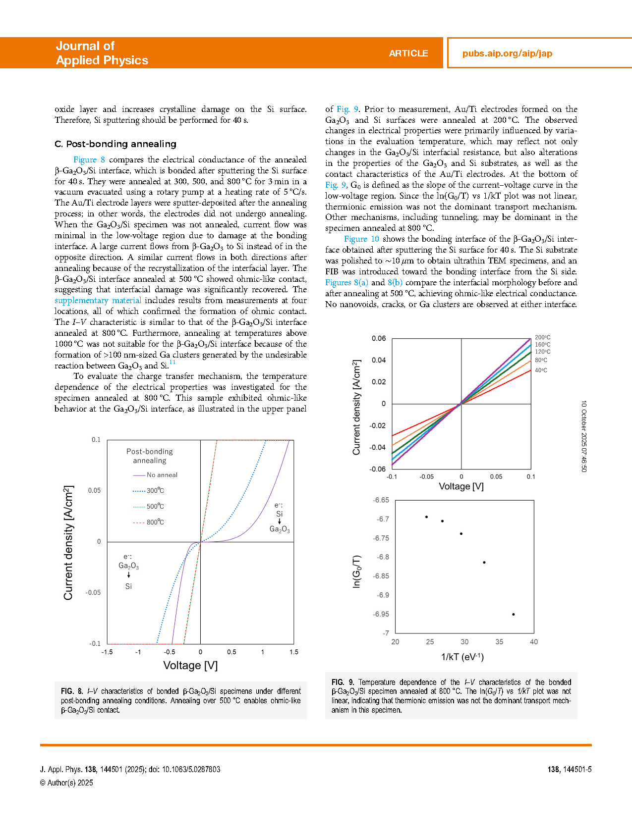
FIG. 8. I–V characteristics of bonded β-Ga2O3/Si specimens under different post-bonding annealing conditions. Annealing over 500 °C enables ohmic-like β-Ga2O3/Si contact.
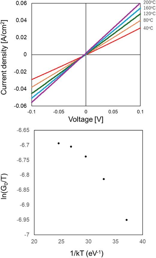
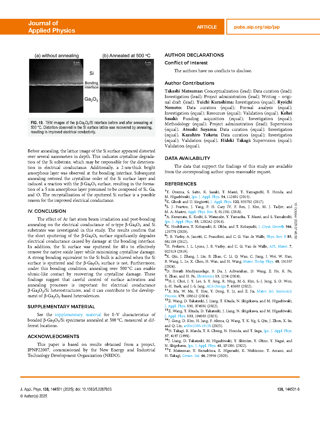
FIG. 9. Temperature dependence of the I–V characteristics of the bonded β-Ga2O3/Si specimen annealed at 800 °C. The ln(G0/T) vs 1/kT plot was not linear, indicating that thermionic emission was not the dominant transport mechanism in this specimen.
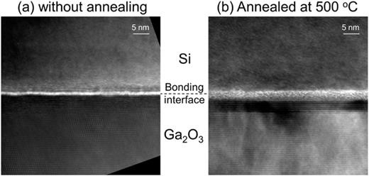
FIG. 10. TEM images of the β-Ga2O3/Si interface before and after annealing at 500 °C. Distortion observed in the Si surface lattice was recovered by annealing, resulting in improved electrical conductivity.
DOI:
doi.org/10.1063/5.0287803