Paper Sharing
【Domestic Papers】Enhanced Breakdown Voltage and Forward Conduction in Dual-Field-Plated β-Ga₂O₃ Lateral Trench Schottky Barrier Diodes
日期:2025-10-29阅读:515
Researchers from the North China University of Technology have published a dissertation titled "Enhanced Breakdown Voltage and Forward Conduction in Dual-Field-Plated β-Ga2O3 Lateral Trench Schottky Barrier Diodes" in Engineering Research Express.
Project Support
This work was supported by the National Natural Science Foundation of China (Grant No.62090054,62404216), the Youth Research Special Project of NCUT (Project No.110051360025XN077-37) and the Scientific Research Initiation Fund Program of NCUT (Project No.11005136025XN076-073).
Background
Monoclinic gallium oxide (β-Ga2O3) has emerged as a highly promising material for power electronic devices, owing to its exceptional material properties including an ultrawide bandgap (~4.8 eV), an exceptionally high theoretical critical electric field strength (~8 MV/cm), and outstanding Baliga's figure of merit (3444). The availability of high-quality β-Ga2O3 single crystals through scalable melt-growth techniques provides distinct advantages over other wide-bandgap semiconductors for high-power applications. β-Ga2O3-based Schottky barrier diodes (SBDs) have attracted considerable research interest due to their combination of low turn-on voltage (Von) and fast switching characteristics, making them particularly suitable for power switching applications. These devices demonstrate superior performance metrics combining high forward current density and excellent reverse blocking capability, positioning them as ideal candidates for demanding high-power applications such as electric vehicle fast-charging systems, high-efficiency industrial motor drives, next-generation power conversion systems.
Abstract
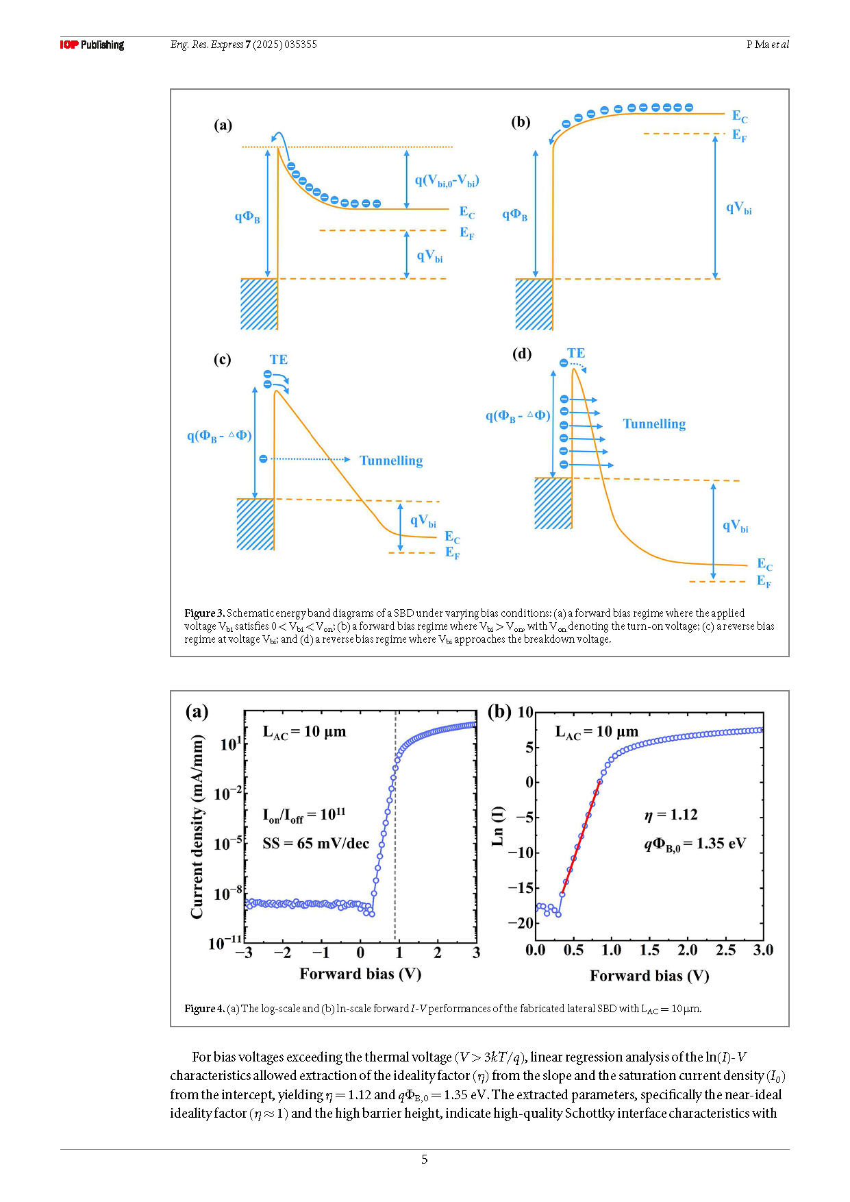
Dual-field-plated β-Ga2O3 lateral Schottky barrier diodes (SBDs) with trench-etched electrodes were developed to mitigate the soft breakdown caused by poor electric field shielding in planar diodes. The trench design simultaneously optimizes field management and enlarges the Schottky contact area, leading to superior forward conduction performance. Device characterization reveals exceptional performance metrics for the 10 μm anode-cathode spacing (LAC) configuration, achieving a record-low specific on-resistance (RON,SP) of 2.0 mΩ·cm², an ultrahigh rectification ratio of 1011, and near-ideal switching behavior with a subthreshold swing (SS) of 65 mV/dec. The extracted ideality factor (η = 1.12) and Schottky barrier height (qΦB,0 = 1.35 eV) confirm the high-quality nature of the fabricated sidewall Schottky interface. The integrated dual field-plate structure, electrically connected to the Schottky contact, demonstrates effective electric field management, enabling a breakdown voltage (VBR) of 1.15 kV at LAC = 35 μm. This corresponds to an impressive power figure of merit (PFOM = VBR2/RON,SP) of 135 MW/cm2, representing one of the highest reported values for β-Ga2O3 single-crystal-based SBDs. These results establish the trench-architecture SBD as a promising candidate for next-generation high-power electronics applications.
Conclusion
This work demonstrates the successful implementation of dual-field-plated β-Ga2O3 lateral trench SBDs that achieve superior forward conduction and reverse blocking characteristics. The trench architecture enables exceptional electrical performance, including a high forward current density of 150 mA/mm, a low RON,SP of 2 mΩ·cm2, an excellent current rectification ratio of 1011. The incorporation of dual field plates effectively mitigates electric field crowding at the Schottky contact, enabling a VBR of 1.15 kV and a corresponding PFOM of 135 MW/cm2. These results underscore the critical role of electric field management at the Schottky interface for device performance optimization. The multiple-field-plate trench architecture emerges as a particularly promising design strategy for high-performance β-Ga2O3 power devices, offering key advantages of full compatibility with standard fabrication processes, enhanced breakdown characteristics, and superior conduction properties. This combination of merits makes the proposed technology especially suitable for next-generation power conversion systems.

Figure 1. (a) HRXRD and (b) AFM characterization images of β-Ga2O3 substrate (c) TEM cross section image of metal/Ga2O3 (d) selected area electron diffraction spectrum of the Ga2O3 layer.

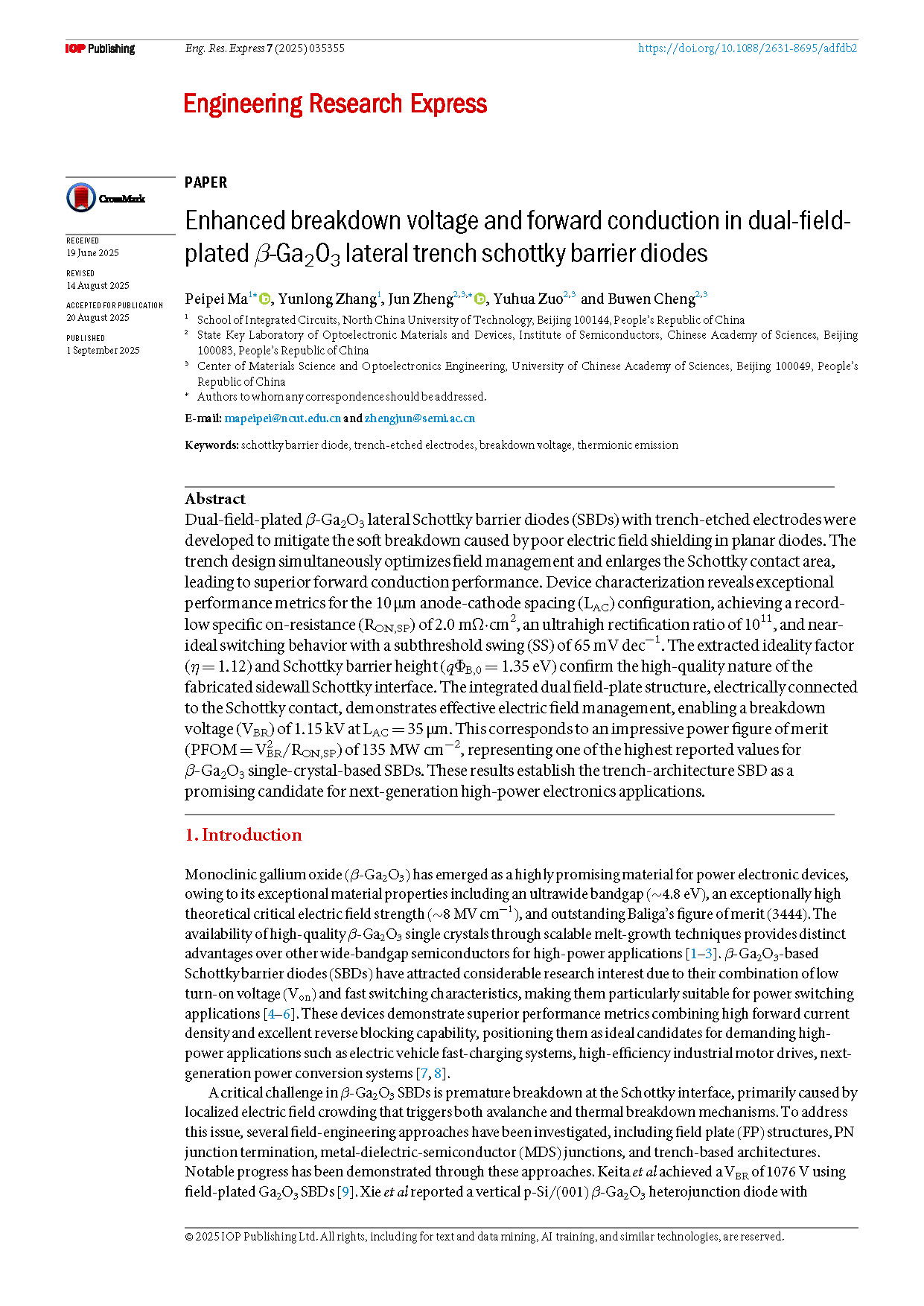
Figure 2. (a) Structure diagram of the fabricated SBD, (b) linear-scale plots of forward I-V and RON,SP-V performances of the fabricated lateral SBDs with LAC = 10 μm and LAC = 35 μm, (c) optical microscopy image of the prepared β-Ga2O3 lateral SBD.
DOI:
doi.org/10.1088/2631-8695/adfdb2