Paper Sharing
【Domestic Papers】High-performance β-Ga₂O₃ solar-blind UV/X-ray photodetector enhanced by oxygen vacancy modulation
日期:2025-10-29阅读:614
Researchers from the University of Science and Technology of China have published a dissertation titled "High-performance β-Ga2O3 solar-blind UV/X-ray photodetector enhanced by oxygen vacancy modulation" in Science China Materials.
Project Support
This work was supported by the National Key Research and Development Program of China (2024YFA1208800 and 2023YFB3610200), the National Natural Science Foundation of China (62304215, 62171426, U23A20358, 62474170 and 62404214), and the funding support from the University of Science and Technology of China (WK2100000056). This work was partially carried out at the National Synchrotron Radiation Laboratory, as well as the Center for Micro and Nanoscale Research and Fabrication of the University of Science and Technology of China.
Background
The wide-bandgap semiconductors, with ultra-wide bandgap, light absorption properties, and robustness in harsh environments, are suitable for ultraviolet and X-ray detection, attracting significant attention in fields such as astronomical exploration, medical imaging, and environmental monitoring. Among these, the ultra-wide-bandgap semiconductor β-Ga2O3 has emerged as one of the most promising candidate materials. With a bandgap of approximately 4.9 eV, the detection spectral range of β-Ga2O3 directly correspond to the solar-blind ultraviolet (SBUV) light without doping adjustments. Extensive research has been conducted on Ga2O3 SBUV detectors, achieving excellent responsivity (R) and SBUV/visible reject ratios. Moreover, due to Ga2O3’s higher X-ray attenuation efficiency compared to Si, preliminary investigations into Ga2O3 direct X-ray detection have been carried out. While the detection performance of Ga2O3 has shown steady improvement through material quality optimization, such as growth process optimization and post-processing, along with advancements in device structure, including heterojunctions and transistors. Recent studies have shown that the high response of Ga2O3 may originate from the Schottky barrier lowering effect and defect-mediated processes.
Abstract
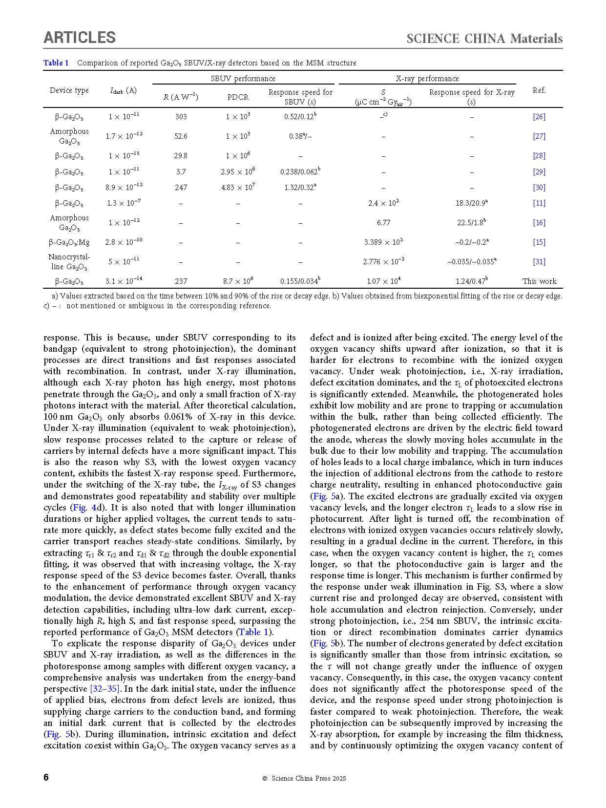
High-performance solar-blind ultraviolet (SBUV) and X-ray detectors are essential for scientific research, medical diagnostics, and astronomical imaging. Ga2O3 has emerged as a promising material for detection in this spectral range. However, the distinct mechanisms underlying SBUV and X-ray detection in Ga2O3 remain poorly understood, hindering the optimization of device performance. This study introduces oxygen vacancy modulation to explore these mechanistic differences and enhance comprehensive detection capabilities of Ga2O3 detectors. Highly crystalline β-Ga2O3 films with different oxygen contents were prepared by metal-organic chemical vapor deposition at various oxygen and trimethylgallium (TEGa) precursor ratios (Foxy/FTEGa), and corresponding detectors were then fabricated. As the Foxy/FTEGa increases, β-Ga2O3 crystal quality improves and oxygen vacancy content decreases. The device based on the film with the lowest oxygen vacancy content exhibits a remarkably low dark current of 30.9 fA. Under SBUV (254 nm), the device demonstrates the photo-to-dark current ratio of 8.7 × 10⁸ and a responsivity of 237 A W−1. Notably, the detector achieves a sensitivity of 10,736 µC cm−2 Gyair−1 under X-rays, which is 477 times higher than that of conventional a-Se detectors. Additionally, the study clarifies the differential roles of oxygen vacancies in the photoresponse under SBUV and X-ray irradiation, offering insights into how these differences affect both responsivity and response speed. These findings not only deepen the understanding of the SBUV and X-ray photoresponse mechanisms in Ga2O3 detectors, but also provide a stepping stone for the design of detectors with excellent comprehensive performance.
Conclusion
In conclusion, MSM photodetectors were fabricated using highly crystalline Ga2O3 thin films, achieving high response to SBUV/X-ray. The study investigated the differences in photocurrent and response speed among devices with different oxygen vacancy contents. Remarkably, due to its high crystal quality and minimal oxygen vacancy content, the device achieved an Idark as low as 30.9 fA. It displayed a remarkable R of 237 A W−1 and a response speed (τr1/τd1) of 155/34 ms under 254 nm SBUV illumination. Moreover, it exhibited outstanding S to X-ray of 10,736 μC cm−2 Gyair−1. The device still maintains stable performance under long-term X-ray irradiation. Guided by energyband analysis under different photoinjection conditions, this work reveals the reasons behind the variations in the photoresponse of Ga2O3 devices. This not only enhances our understanding of the mechanisms governing the photoresponse to SBUV/X-ray in Ga2O3, but also is crucial for advancing the design and engineering of future high-performance optoelectronic devices.
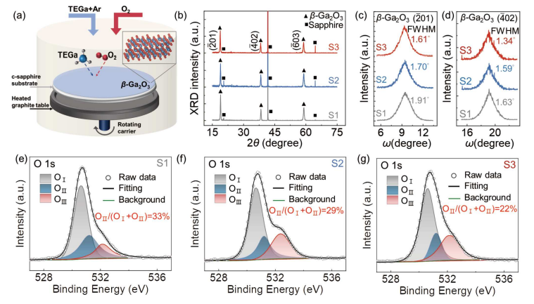
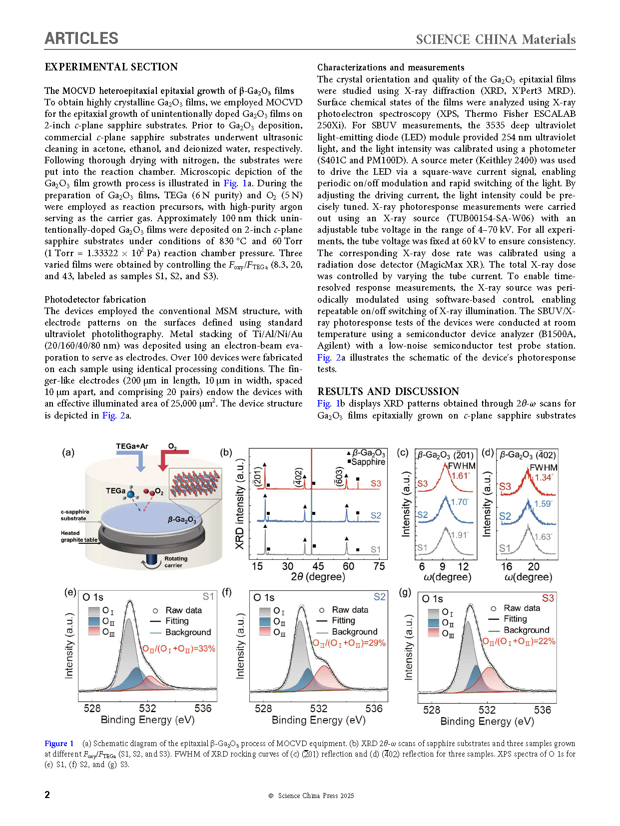
Figure 1 (a) Schematic diagram of the epitaxial β-Ga2O3 process of MOCVD equipment. (b) XRD 2θ-ω scans of sapphire substrates and three samples grown at different Foxy/FTEGa (S1, S2, and S3). FWHM of XRD rocking curves of (c) (-201) reflection and (d) (-402) reflection for three samples. XPS spectra of O 1s for (e) S1, (f) S2, and (g) S3.
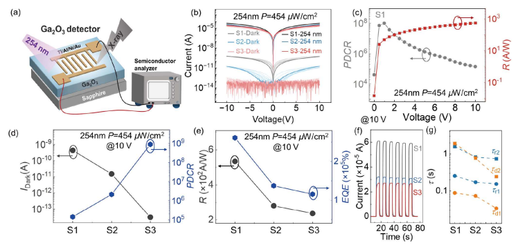
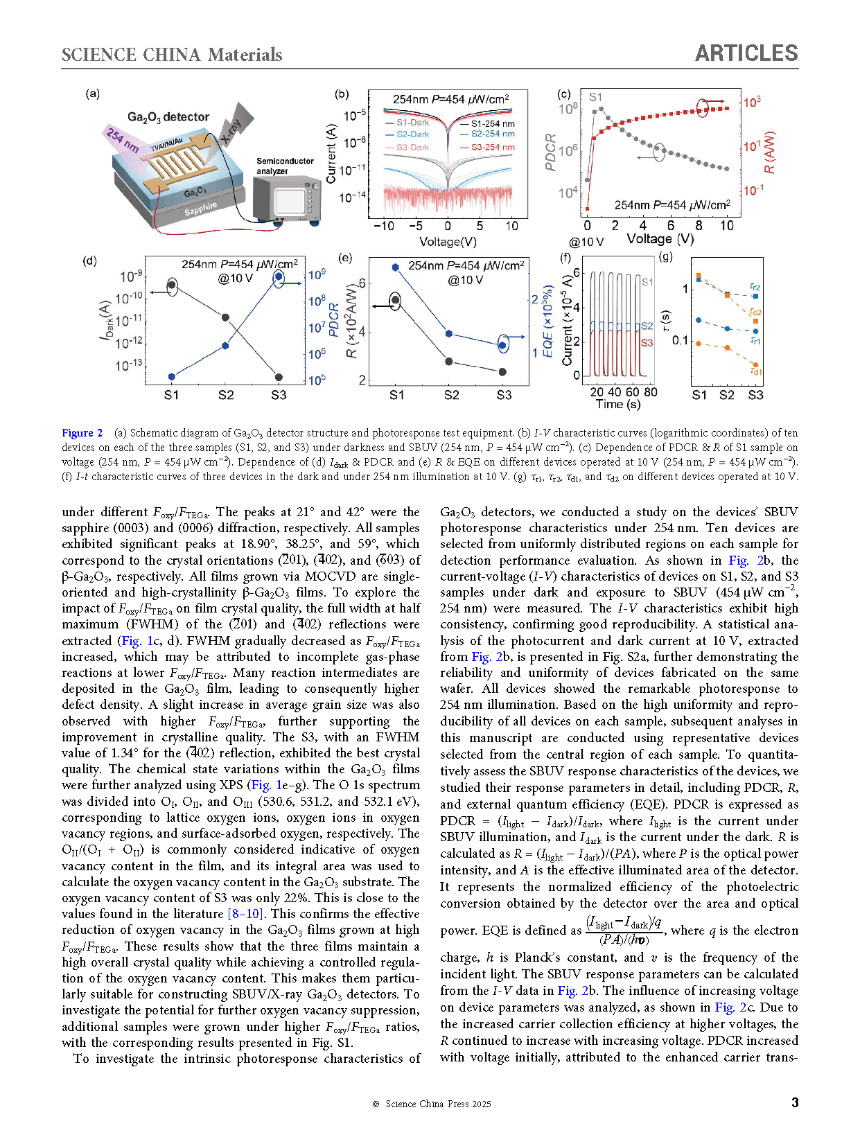
Figure 2 (a) Schematic diagram of Ga2O3 detector structure and photoresponse test equipment. (b) I-V characteristic curves (logarithmic coordinates) of ten devices on each of the three samples (S1, S2, and S3) under darkness and SBUV (254 nm, P = 454 μW cm−2). (c) Dependence of PDCR & R of S1 sample on voltage (254 nm, P = 454 μW cm−2). Dependence of (d) Idark & PDCR and (e) R & EQE on different devices operated at 10 V (254 nm, P = 454 μW cm−2). (f) I-t characteristic curves of three devices in the dark and under 254 nm illumination at 10 V. (g) τr1, τr2, τd1, and τd2 on different devices operated at 10 V.
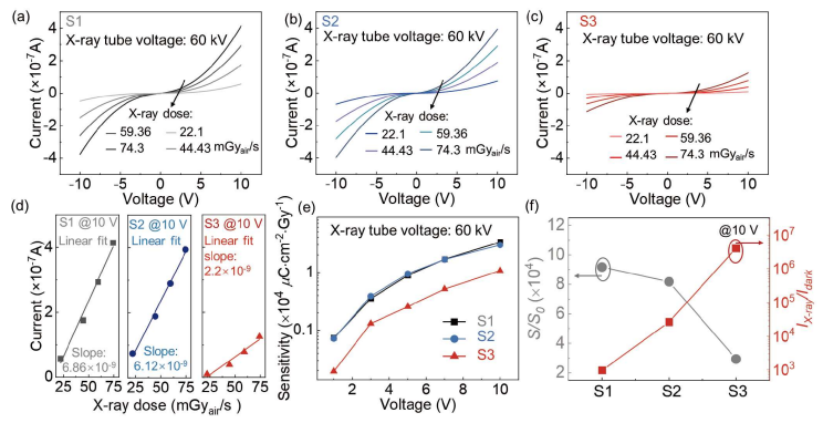
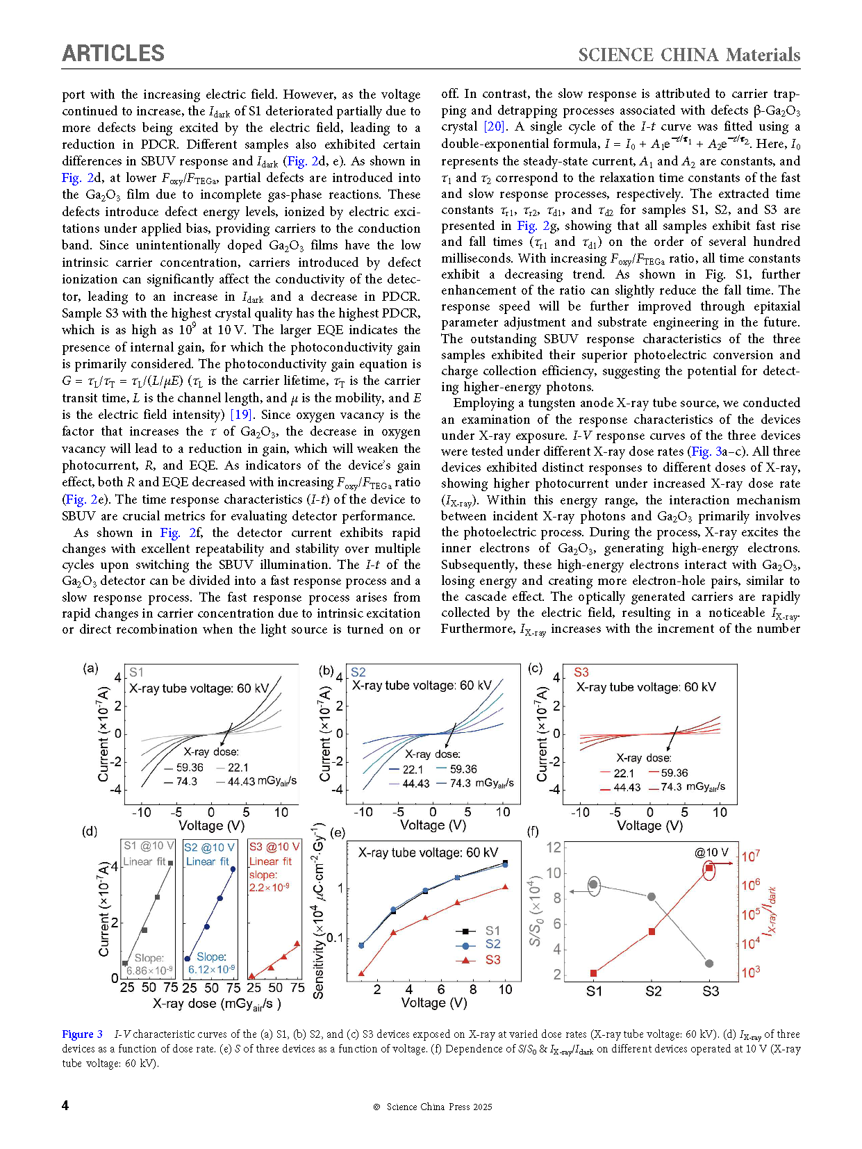
Figure 3 I-V characteristic curves of the (a) S1, (b) S2, and (c) S3 devices exposed on X-ray at varied dose rates (X-ray tube voltage: 60 kV). (d) IX-ray of three devices as a function of dose rate. (e) S of three devices as a function of voltage. (f) Dependence of S/S0 & IX-ray/Idark on different devices operated at 10 V (X-ray tube voltage: 60 kV).

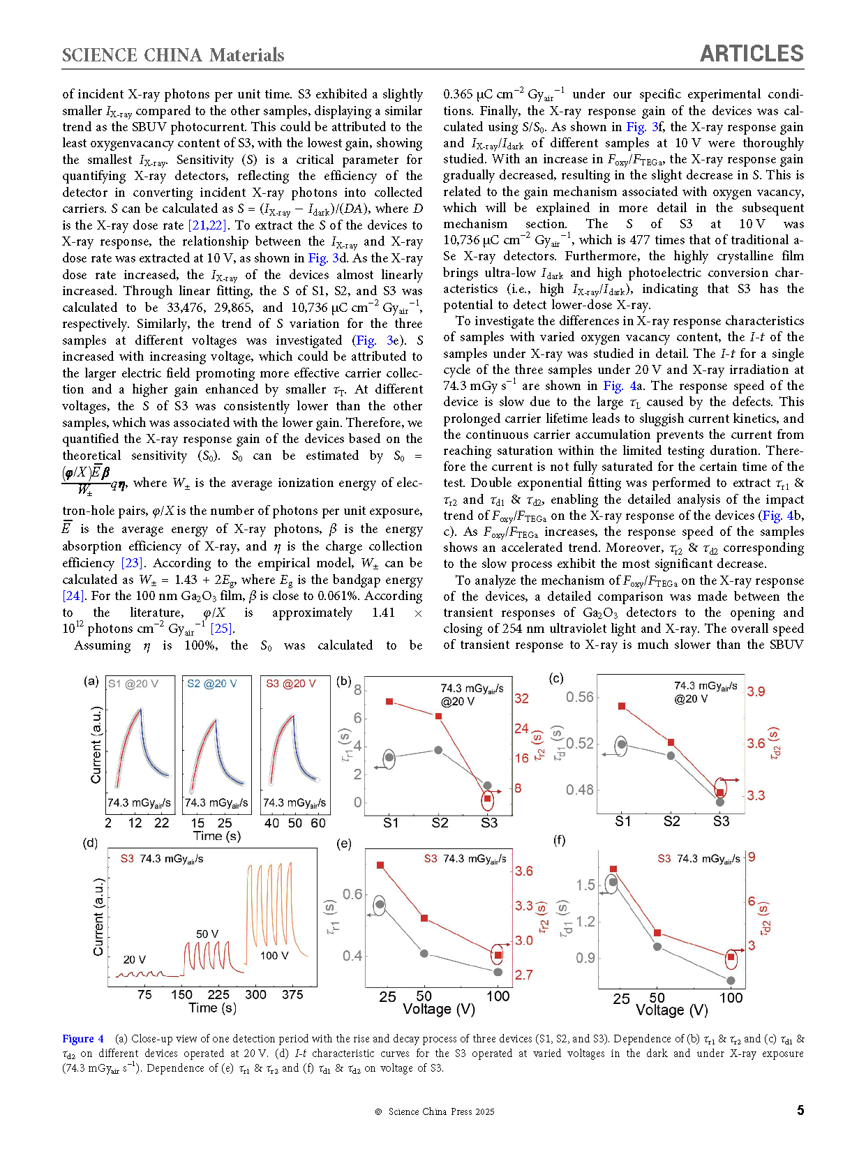
Figure 4 (a) Close-up view of one detection period with the rise and decay process of three devices (S1, S2, and S3). Dependence of (b) τr1 & τr2 and (c) τd1 & τd2 on different devices operated at 20 V. (d) I-t characteristic curves for the S3 operated at varied voltages in the dark and under X-ray exposure (74.3 mGyairs−1). Dependence of (e) τr1 & τr2 and (f) τd1 & τd2 on voltage of S3.
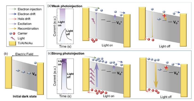
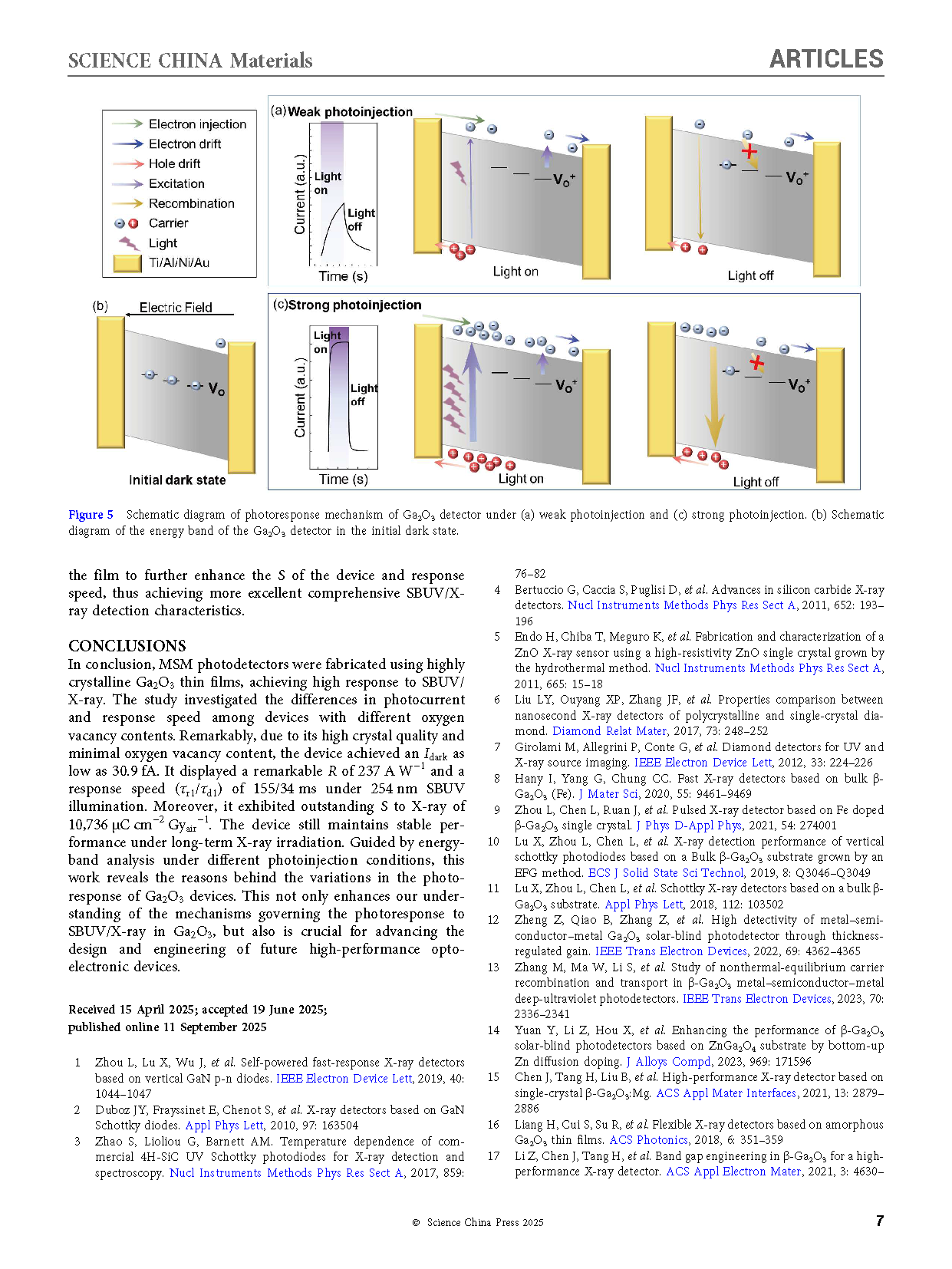
Figure 5 Schematic diagram of photoresponse mechanism of Ga2O3 detector under (a) weak photoinjection and (c) strong photoinjection. (b) Schematic diagram of the energy band of the Ga2O3 detector in the initial dark state.
DOI:
doi.org/10.1007/s40843-025-3495-8