Paper Sharing
【Member Papers】Performance and Stability Improvements in β-Ga₂O₃ MOSFET With Thin HfAlO Gate Dielectric by O₂ Plasma Treatment
日期:2025-10-29阅读:580
A research team from Xiamen University has published a paper titled "Performance and Stability Improvements in β-Ga2O3 MOSFET With Thin HfAlO Gate Dielectric by O2 Plasma Treatment" in the academic journal IEEE Transactions on Electron Devices.
Project Support
This work was supported by the National Natural Science Foundation of China (Grant No. 62171396) and the Shenzhen Basic Research Program (Grant No. JCYJ20240813145617023).
Background
Beta-phase gallium oxide (β-Ga₂O₃), recognized as a key material for next-generation high-power electronic devices, exhibits an ultra-wide bandgap (~4.9 eV), an extremely high critical breakdown field strength (8 MV/cm), and potential for low-cost substrate fabrication. However, the material system faces two major challenges: first, the instability of the threshold voltage caused by gate dielectric interface defects severely limits device reliability; second, the mainstream (010) plane substrates encounter bottlenecks in large-size, low-cost manufacturing. To address these issues, this study explores the more challenging (100) plane substrate, which is more suitable for large-area fabrication despite its inferior epitaxial quality. This paper reports the full-process technology chain—from molecular beam epitaxy (MBE) material growth and device fabrication to systematic performance testing—on a (100) plane Fe-doped semi-insulating β-Ga₂O₃ substrate. By implementing O2 plasma treatment on the HfAlO gate dielectric, high-performance and highly reliable MOSFETs have been successfully achieved, providing new technical options and experimental support for the industrialization of β-Ga₂O₃.
Main Content
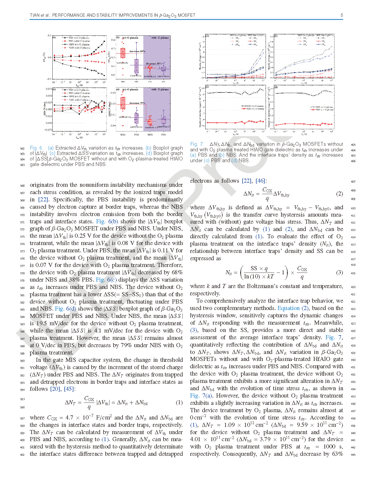
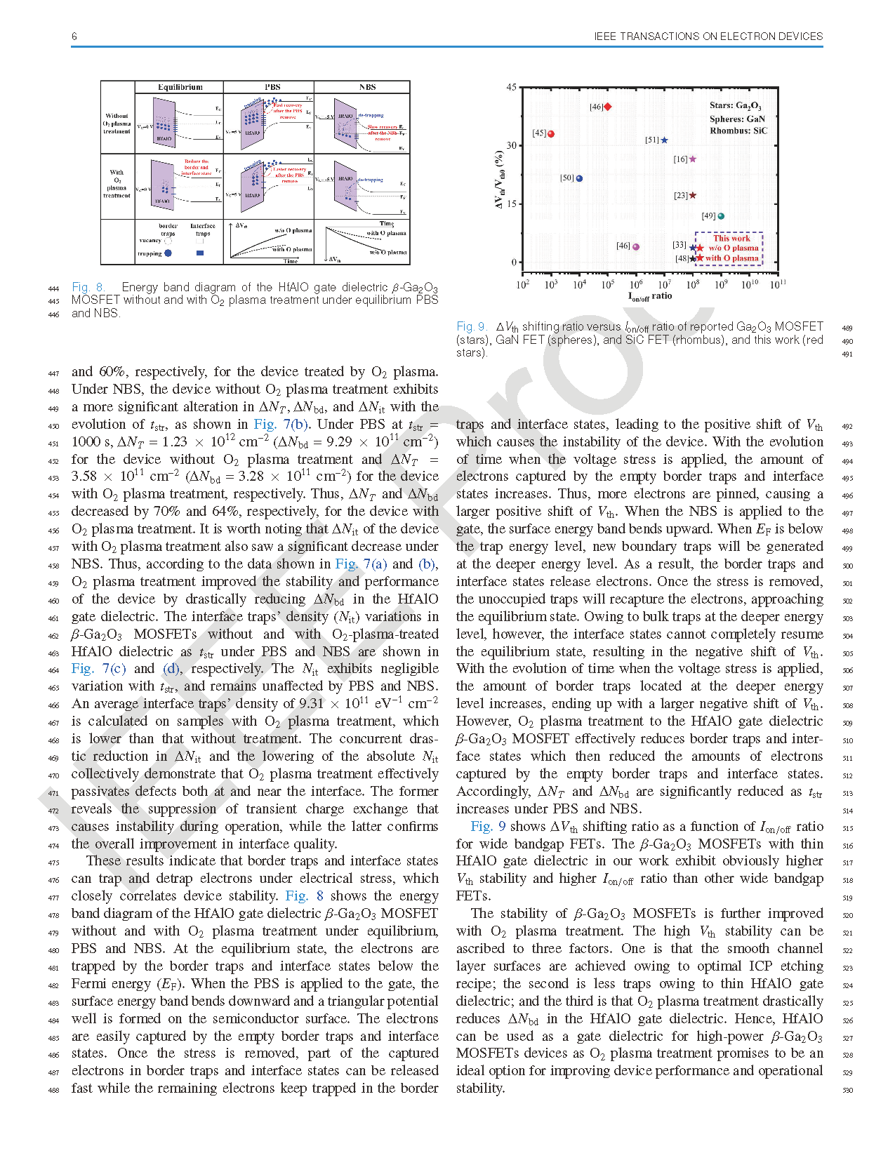
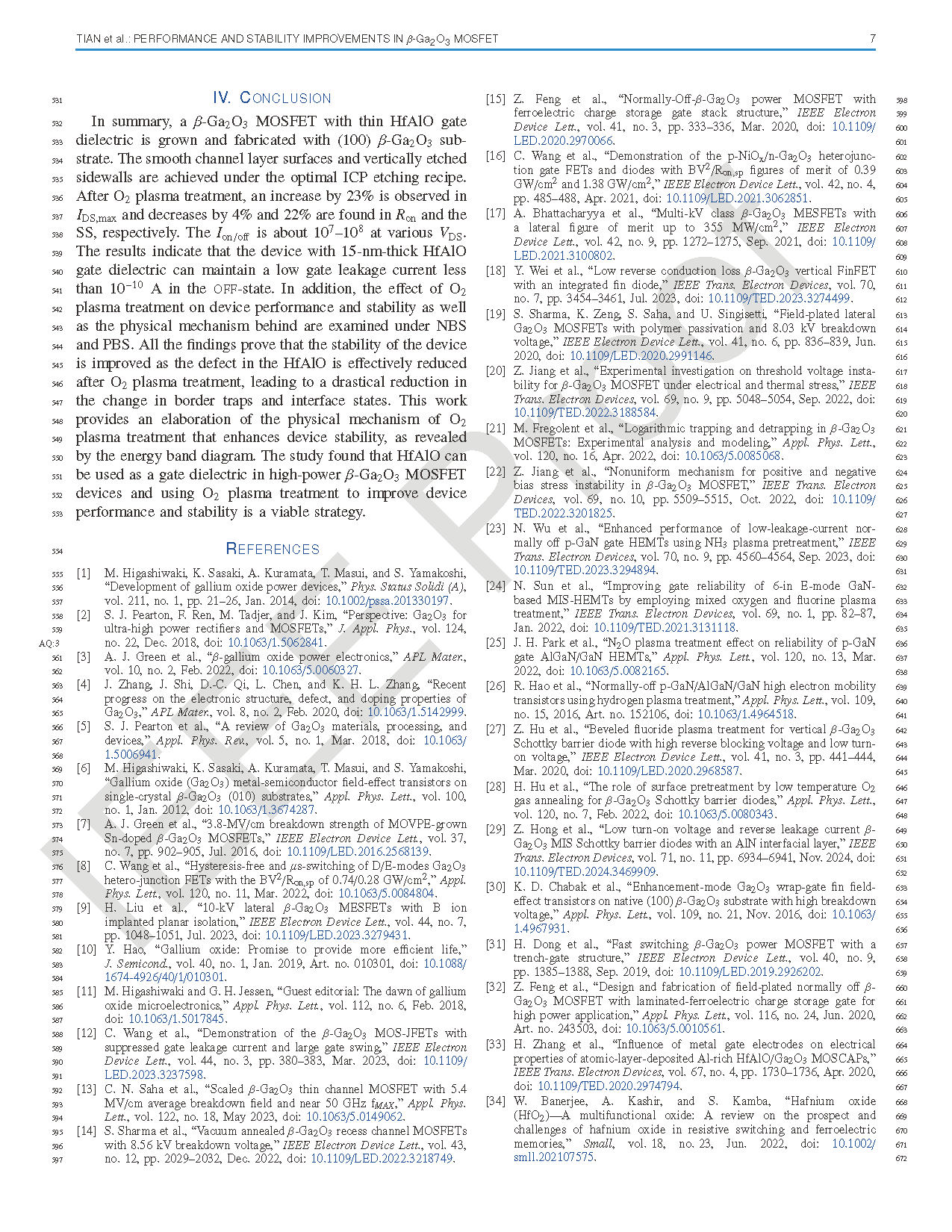
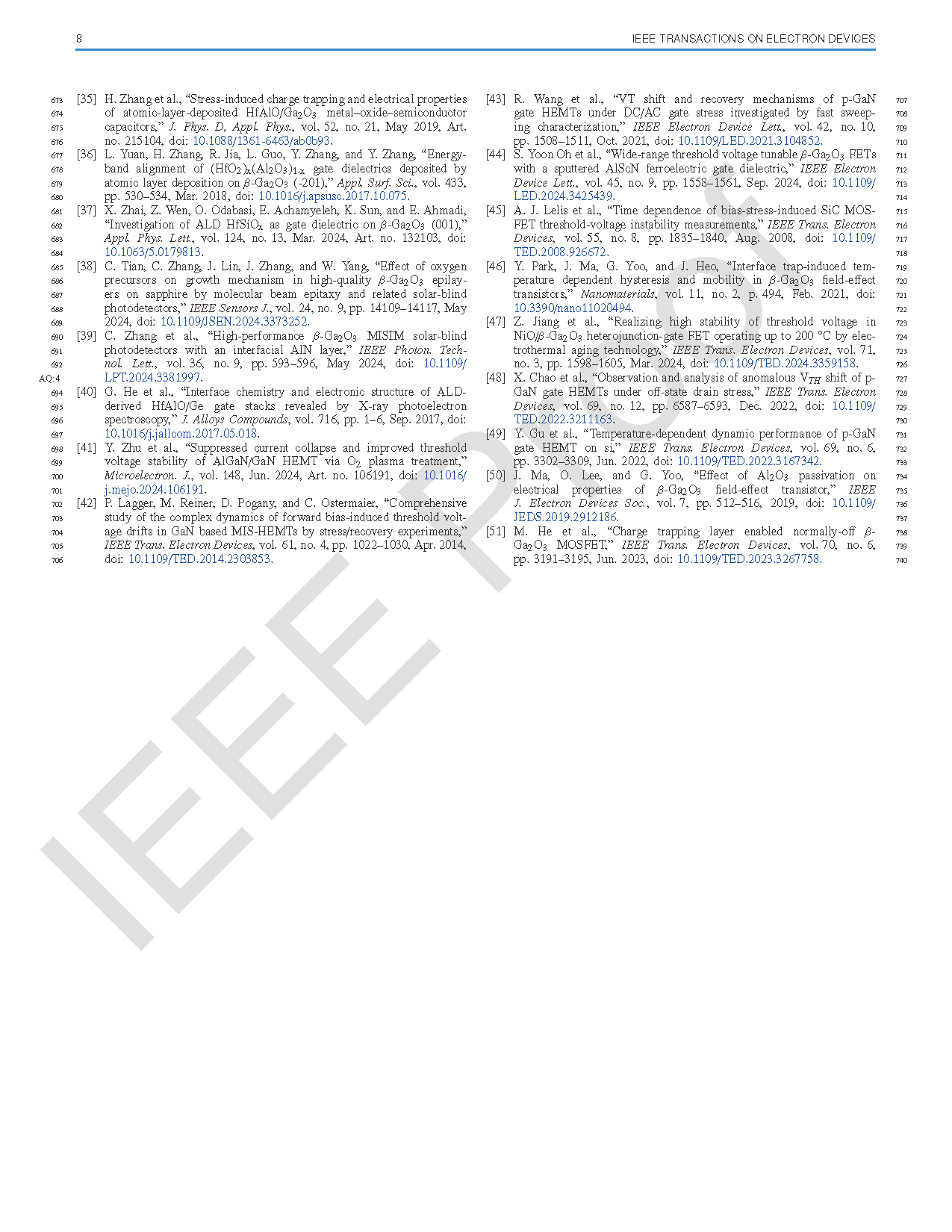
The research team successfully grew high-quality epitaxial layers on a (100) plane β-Ga₂O₃ substrate using molecular beam epitaxy (MBE). Subsequently, an optimized inductively coupled plasma (ICP) etching process was employed to achieve an atomic-level channel surface with a roughness as low as 0.457 nm, laying a solid foundation for high-performance devices. The device utilized a 15 nm HfAlO high-k material as the gate dielectric, achieving excellent gate control capability and low gate leakage current (<10-10 A). Through O2 plasma treatment of the HfAlO gate dielectric, interface and bulk defects were effectively repaired, reducing electron trap centers. After O2 plasma treatment, the maximum drain current (IDS,max) increased by 23%, the subthreshold swing (SS) decreased by 22%, and the on/off current ratio (Ion/off) reached 108. The impact of O2 plasma treatment on device stability was systematically investigated through positive/negative bias stress (PBS/NBS) tests: after treatment, under NBS conditions, the threshold voltage variation (|ΔVth|) decreased from 0.25 V to 0.08 V, and the subthreshold swing variation (|ΔSS|) decreased from 0.02 V/dec to 0.004 V/dec, representing reductions of 68% and 79%, respectively, fully validating the stability enhancement effect. The physical mechanisms were further elucidated by combining energy band structure diagrams under different states (equilibrium, PBS, NBS). The study demonstrates that O2 plasma treatment effectively suppresses border traps and interface state density, reducing the number of electron trapping/de-trapping events, specifically manifested as a significant attenuation in the variation of border trap and interface state charges, thereby enhancing device stability.
Summary
The research team successfully established a full-process technology chain for β-Ga₂O₃ MOSFET devices, encompassing MBE epitaxial growth, device fabrication, and performance and stability testing. Through systematic bias stress tests and quantitative analysis of trap density, the fundamental reasons for performance improvement were revealed at the physical mechanism level. The study shows that O2 plasma treatment effectively suppresses border trap density and interface state charge trapping in the gate dielectric, significantly reducing the probability of electron trapping/de-trapping, thereby fundamentally improving the threshold voltage stability of the device. This work not only verifies the application potential of HfAlO as a gate dielectric in high-power β-Ga₂O₃ MOSFETs but also provides a feasible technical path and theoretical basis for achieving high-performance gallium oxide devices on large-size, low-cost (100) plane substrates.

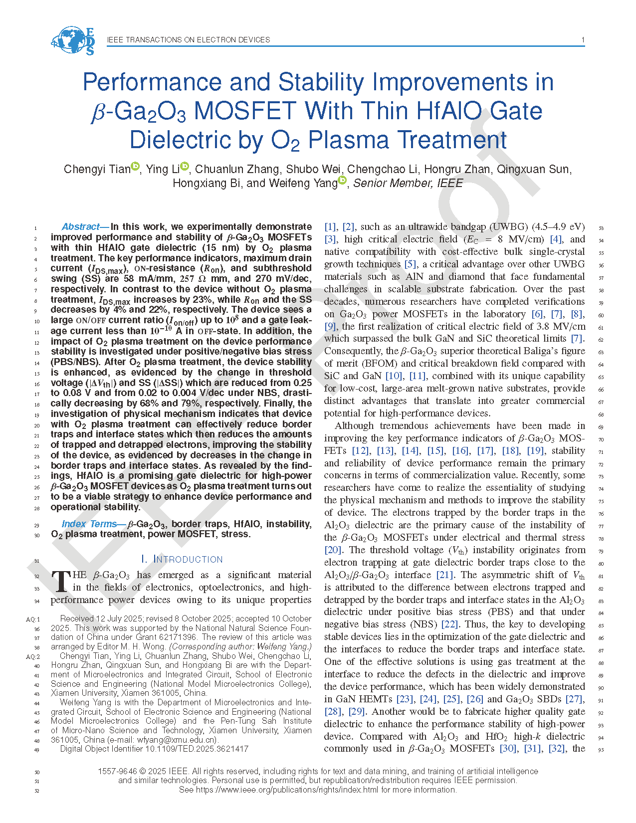
FIG.1 (a) Cross-sectional schematic view of the β-Ga2O3 MOSFET with thin HfAlO gate dielectric. (b) β-Ga2O3 MOSFET device fabrication flow. (c) Cross-sectional view of etch depth of ohmic cap layer and AFM image of the channel layer surface (inset). (d) Top-view optical image of the fabricated β-Ga2O3 MOSFET. (e) XRD spectra for HfAlO samples grown on sapphire substrate, with and without O2 plasma treatment (Inset: AFM of HfAlO). (f) XPS spectra of Al 2p and O 1s peaks for HfAlO samples, with and without O2 plasma treatment.

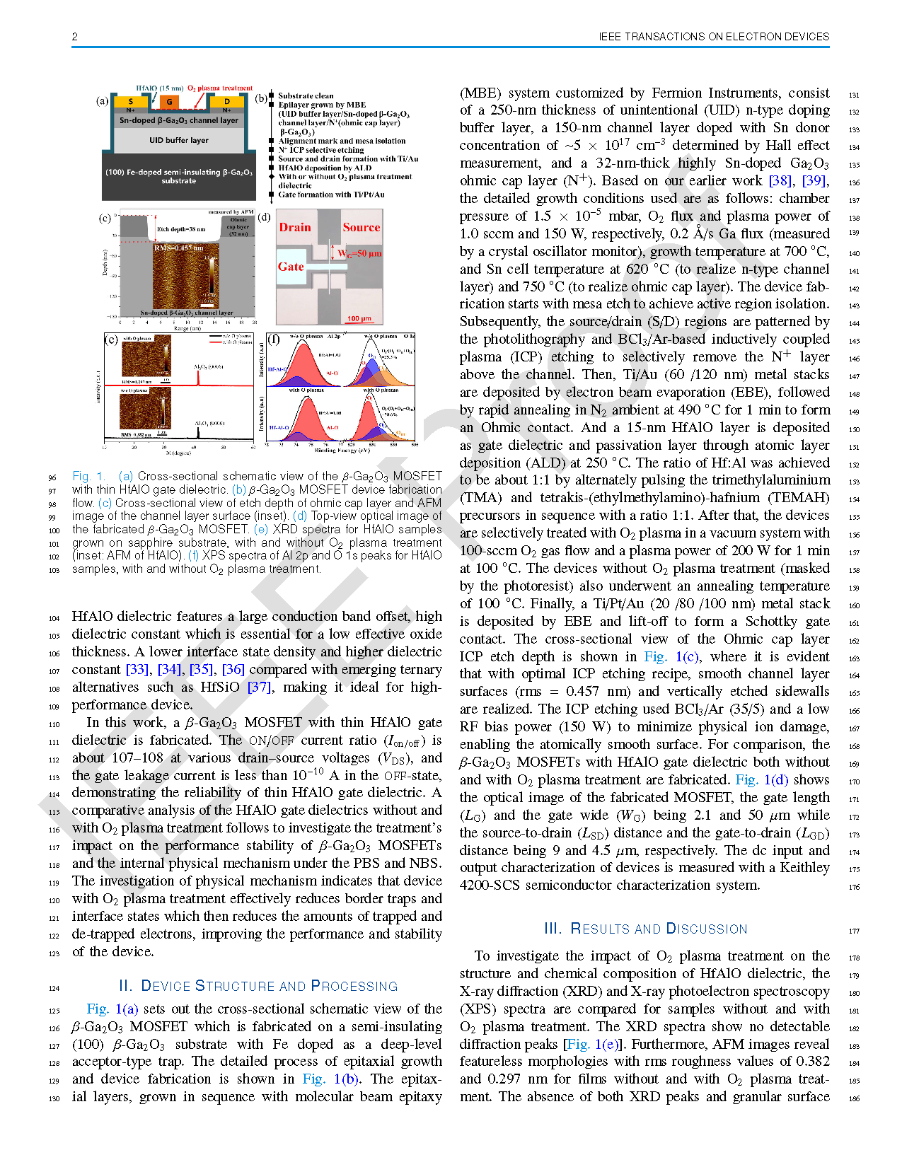
FIG.2 (a) Output characteristics and (b) linear and log scale transfer characteristics of β-Ga2O3 MOSFET without (w/o) and with O2 plasma treatment of the HfAlO gate dielectric.

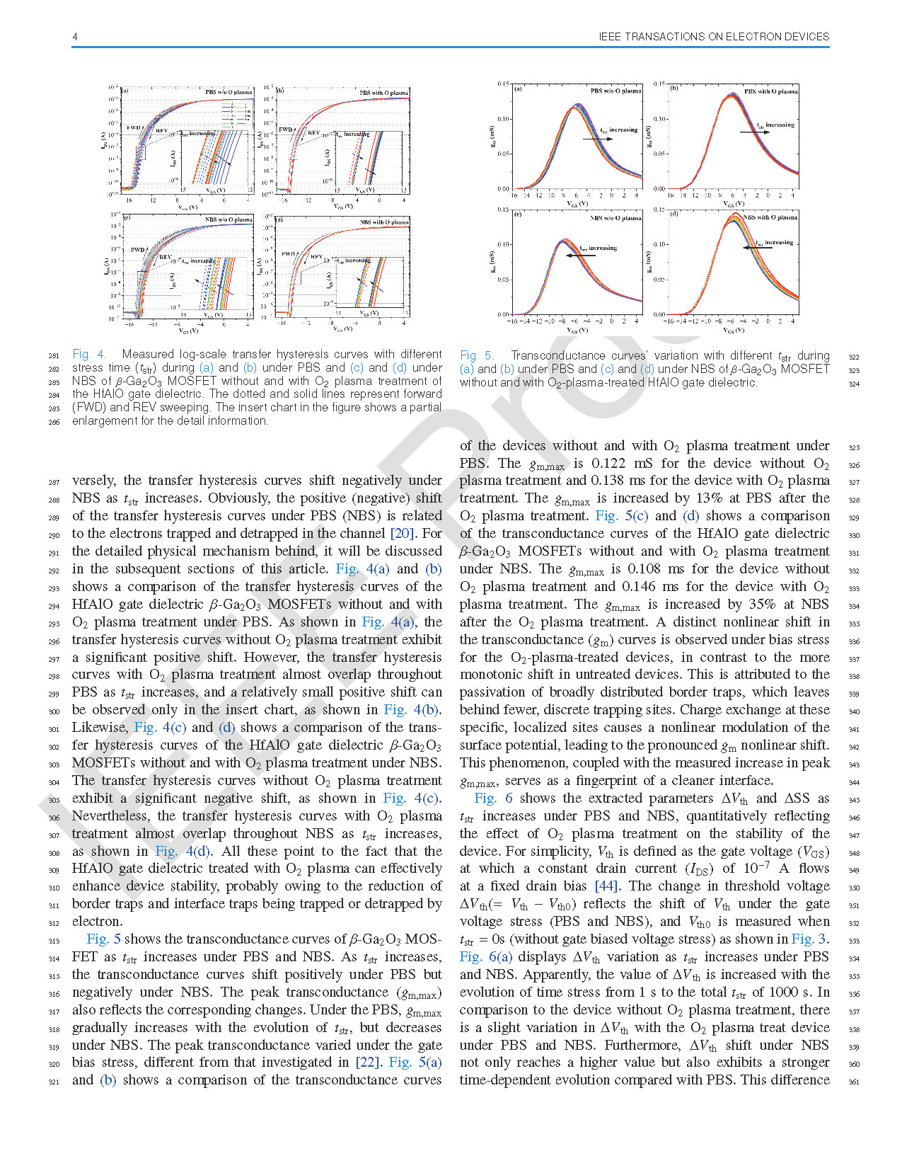
FIG.3 Measured log-scale transfer hysteresis curves with different stress time (tstr) during (a) and (b) under PBS, (c) and (d) under NBS of β-Ga2O3 MOSFET without and with O2 plasma treatment of the HfAlO gate dielectric. The dotted and solid lines represent forward (FWD) and reverse (REV) sweeping. The insert chart in the figure shows a partial enlargement for the detail information.
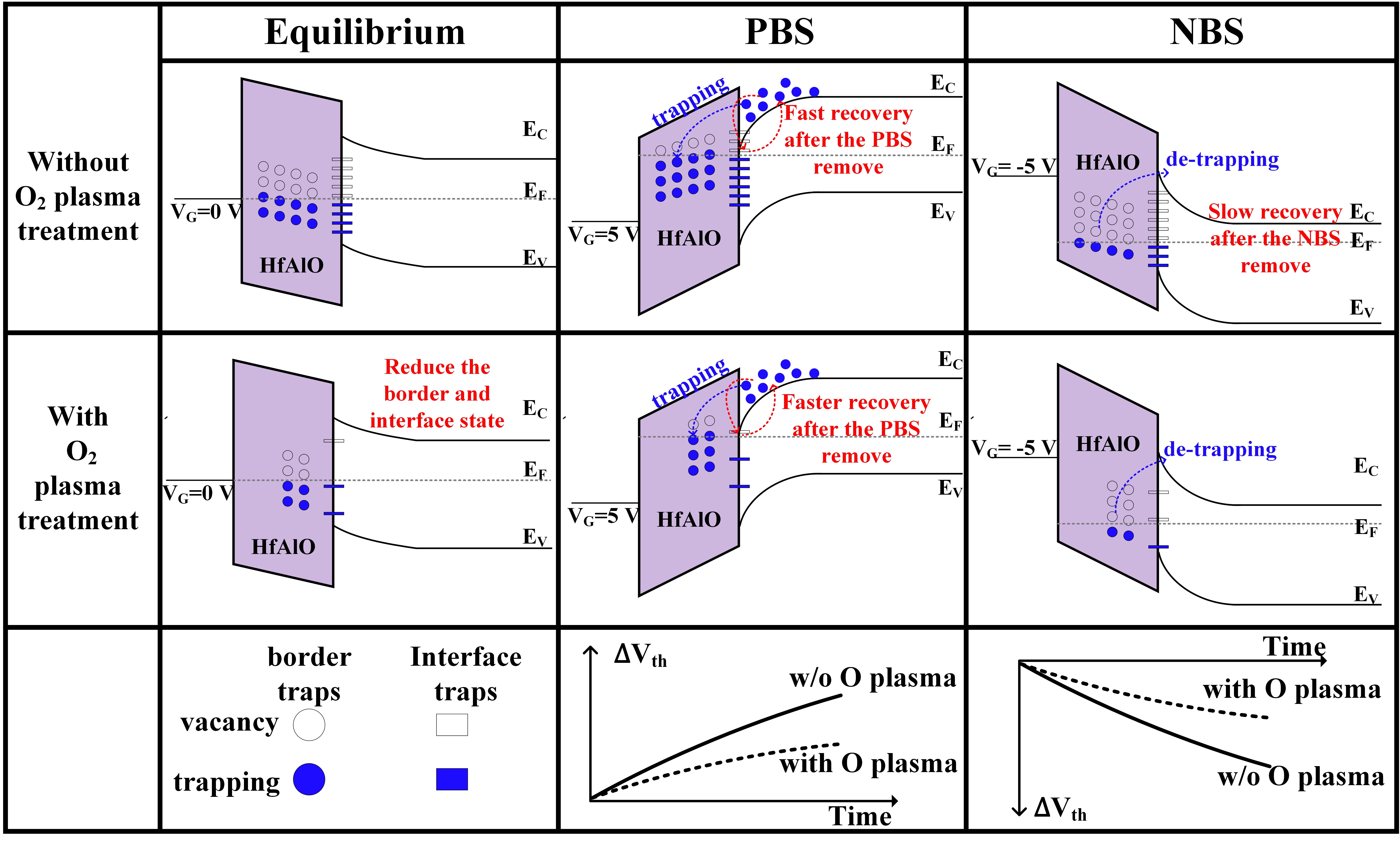
FIG.4. Energy band diagram of the HfAlO gate dielectric β-Ga2O3 MOSFET without and with O2 plasma treatment under equilibrium, PBS and NBS.
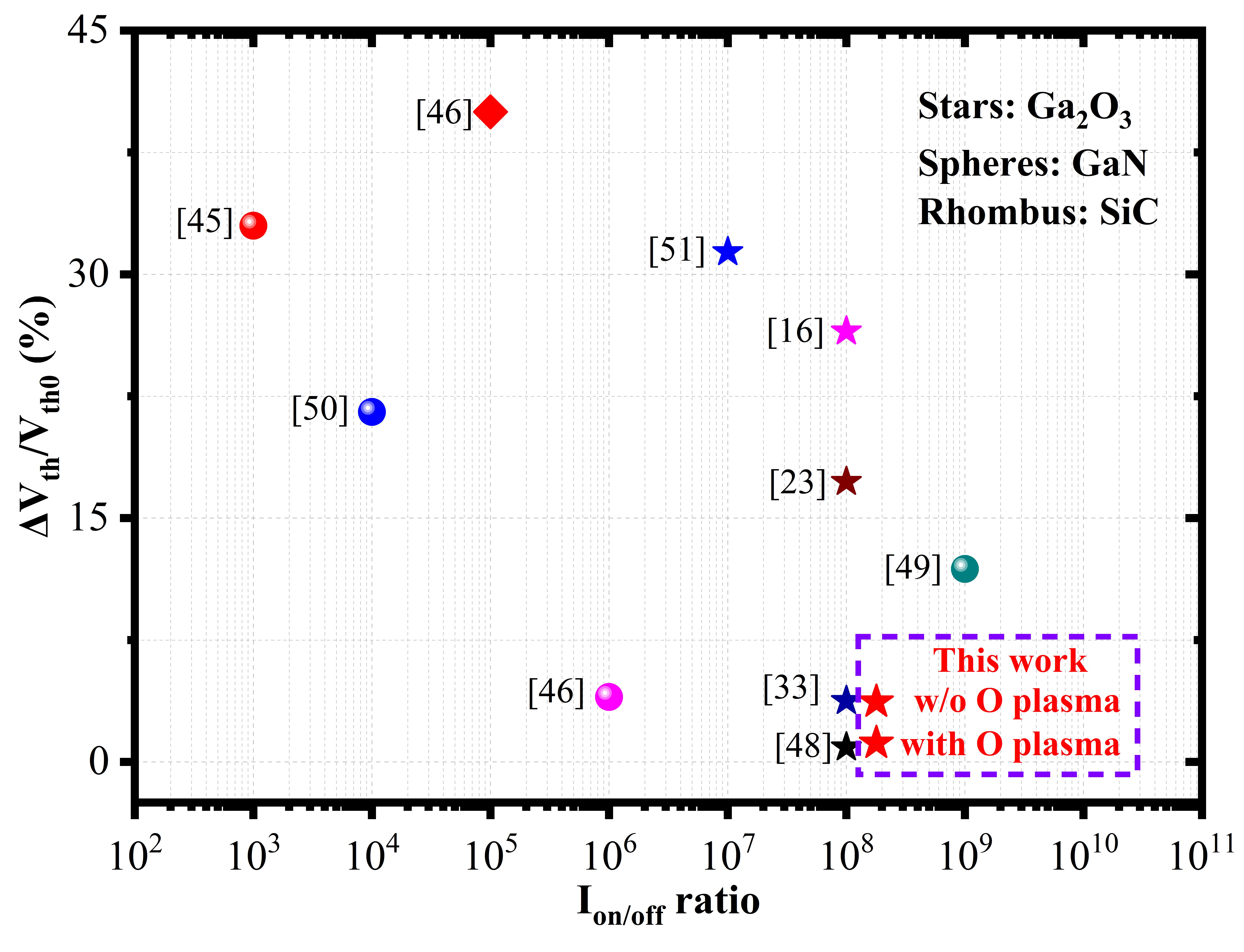
FIG.5 The ∆Vth shifting ratio versus the Ion/off ratio of reported Ga2O3 MOSFET (stars), GaN FET (spheres) and SiC FET (rhombus) and this work (red stars).
DOI:
10.1109/TED.2025.3621417