Paper Sharing
【Domestic Papers】Localized Surface Plasmon Resonance-Driven 71.9 % EQE in Ga₂O₃ Photodetectors: From Photovoltaic Enhancement to Multifunctional Optoelectronic Logic Gates Integration
日期:2025-10-30阅读:556
Researchers from the Guangdong University of Technology have published a dissertation titled "Localized Surface Plasmon Resonance-Driven 71.9 % EQE in Ga2O3 Photodetectors: From Photovoltaic Enhancement to Multifunctional Optoelectronic Logic Gates Integration" in Materials Today Physics.
Project Support
This work was financially supported by the Open Research Fund of Songshan Lake Materials Laboratory [grant number 2023SLABFK01], Guangzhou Science and Technology Program [grant number 2025A04J3852], the National Natural Science Foundation of China [grant numbers 62004229, 62204270], and Fujian Provincial Natural Science Foundation Project [grant number 2024J01251].
Background
Logic gates, the fundamental building blocks of modern digital computers and logic circuits, enable complex information processing by performing Boolean algebra operations on binary digits (0 and 1). Among these, optoelectronic logic gates (OELGs) have emerged as a pioneering class of devices that integrate light signals and electronic components to execute logical operations. Leveraging the unique advantages of light signals, such as high transmission speed and parallel computing capabilities, OELGs hold significant promise for communication applications.
Early OELGs were limited to single logic functions implemented in individual devices. However, recent breakthroughs have enabled the integration of multiple logic functions within one device. Compared with traditional OELGs, these multifunctional OELGs not only improve system integration and reduce costs but also enhance operational flexibility. As a result, they have become a central focus of current research and are widely regarded as a key technology for advancing digital computing and communication.
Abstract
Ga2O3-based photodetectors with dual-band response characteristics hold great promise for realizing multifunctional optoelectronic logic gates (OELGs) in digital computing and secure communication. In this work, a hybrid organic-inorganic heterojunction based on PEDOT:PSS/Pt NPs/Ga2O3/GaN is designed to overcome the zero-bias performance bottleneck of conventional Ga2O3 heterojunction photodetectors and to integrate multiple logic operations into a single device. Under 254 nm illumination and 0 V bias, the device achieves an ultra-high external quantum efficiency (EQE) of ∼71.9% via the localized surface plasmon resonance (LSPR) of platinum (Pt) nanoparticles (NPs) embedded at the PEDOT:PSS/Ga2O3 interface. Statistics from twelve additional devices yield a median EQE of 71.3%. When an external bias is applied, the photodetector exhibits a tunable dual-band response in the UVC and UVA regions. By programming the bias voltage and optical inputs, six reconfigurable logic functions (NOR, NOT, NAND, XNOR, OR, and AND) are realized within a single unit, demonstrating its potential for parallel optical computing. Additionally, an encryption communication system based on these OELGs validates their applicability in secure data transmission, where dual-band signals can be dynamically encoded and decoded.
Highlights
● An organic-inorganic hybrid Ga2O3detector is designed with Pt nanoparticles (NPs).
● The LSPR effect of Pt NPs is key to improved performance.
● Six logic operations are realized within a single Ga2O3
● An encryption-decryption process is demonstrated in Ga2O3optoelectronic logic gate.
Conclusion
In summary, embedding Pt NPs at the PP/Ga2O3 interface of the PP-Pt/Ga2O3/GaN photodetector induces a LSPR effect, which enhances light harvesting and carrier dynamics. This results in a high D* of ∼5.4 × 10¹¹ Jones, a responsivity of 148.30 mA W−1, and an EQE of 71.9 % under 0 V operation.The LSPR effect contributed by the Pt NPs is not limited to zero-bias enhancement but acts as a persistent performance booster across the operational voltage range. These superior metrics enable the implementation of six reconfigurable logic functions within a single optical-electronic logic gate (OELG). By modulating the external bias to tailor the energy band alignment and illumination condition, NOR, NOT, NAND, XNOR, OR, and AND logic operations are achieved. The synergy between plasmonic enhancement and bias-controlled carrier dynamics thus paves the way for on-chip optical computing in a single device. Practical demonstrations of encrypted communication protocols based on this logic gate further validate its potential for secure data transmission systems. These results not only highlight the promise of Ga2O3-based heterojunctions for low-power multifunctional optoelectronics but also provide innovative design strategies for nextgeneration high-performance logic devices.
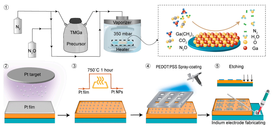
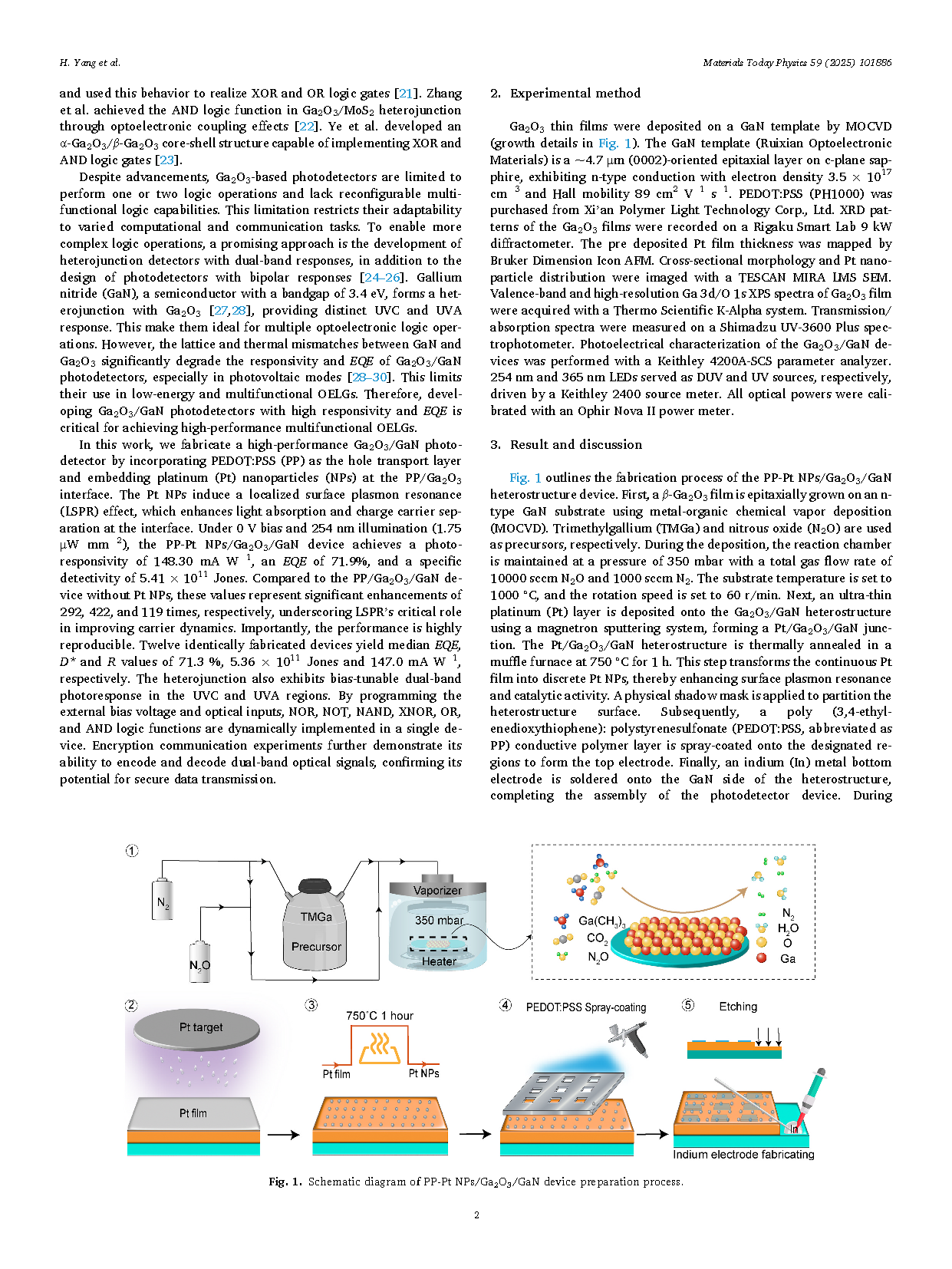
Fig. 1. Schematic diagram of PP-Pt NPs/Ga2O3/GaN device preparation process.
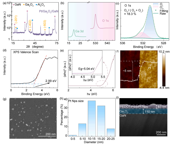
Fig. 2. (a) XRD pattern of β-Ga2O3 film deposited on n-GaN. (b) High-resolution XPS spectra of Ga 3d and O 1s core levels. (c) High-resolution XPS spectrum of the O 1s (core level) along with its peak deconvolution results. (d) XPS valence band scan spectrum of the β-Ga2O3 film. (e) Absorption spectrum of the Ga2O3 film. The band gap estimation outcome is shown in the inset. (f) AFM topography image and line profile analysis of the Pt/Si stepped structure. (g) SEM image of Pt NPs derived from thermally annealed Pt thin film at 750 °C. (h) Size statistics of the NPs. (i) Cross-sectional SEM image of PP-Pt NPs/Ga2O3/GaN heterojunction.
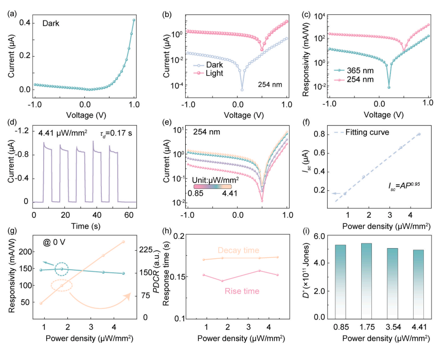
Fig. 3. (a) I-V characteristics of PP-Pt/Ga2O3/GaN device in the dark. The inset is the schematic diagram of the device. (b) I-V curves of the device under UVC illumination and dark conditions. (c) Responsivity (R) of the device under 365 nm and 254 nm illumination at different bias voltages. (d) Multi-cycle I-T curve at 0 V bias and under periodic UVC illumination (4.41 μW mm−2). (e) I-V curves under UVC illumination with varying optical power. (f) ISC vs optical power density. (g) Responsivity and PDCR dependence on optical power density. (h) Variation of decay time and rise time with optical power density. (i) Relationship between D* and optical power density.
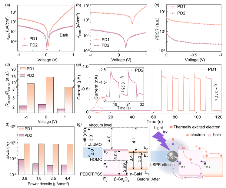
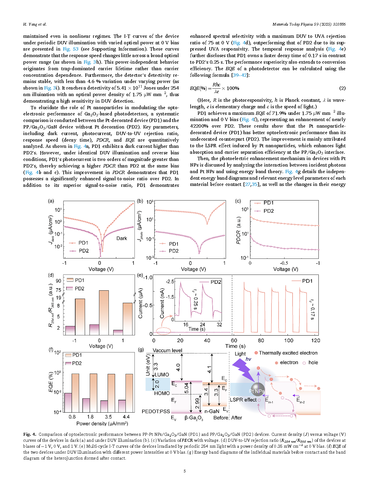
Fig. 4. Comparison of optoelectronic performance between PP-Pt NPs/Ga2O3/GaN (PD1) and PP/Ga2O3/GaN (PD2) devices. Current density (J) versus voltage (V) curves of the devices in dark (a) and under DUV illumination (b). (c) Variation of PDCR with voltage. (d) DUV-to-UV rejection ratio (R254nm/R365nm) of the devices at biases of − 1 V, 0 V, and 1 V. (e) Multi-cycle I-T curves of the devices irradiated by periodic 254 nm light with a power density of 0.35 mW cm−2 at 0 V bias. (f) EQE of the two devices under DUV illumination with different power intensities at 0 V bias. (g) Energy band diagrams of the individual materials before contact and the band diagram of the heterojunction formed after contact.

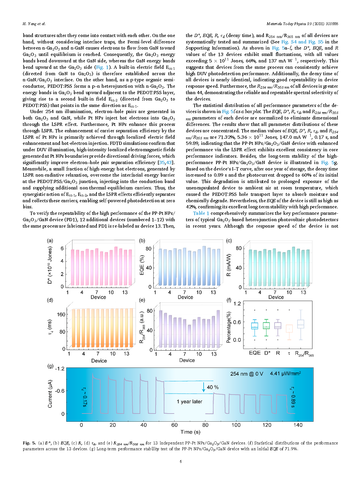
Fig. 5. (a) D*, (b) EQE, (c) R, (d) τd, and (e) R254 nm/R365 nm for 13 independent PP-Pt NPs/Ga2O3/GaN devices. (f) Statistical distributions of the performance parameters across the 13 devices. (g) Long-term performance stability test of the PP-Pt NPs/Ga2O3/GaN device with an initial EQE of 71.9%.
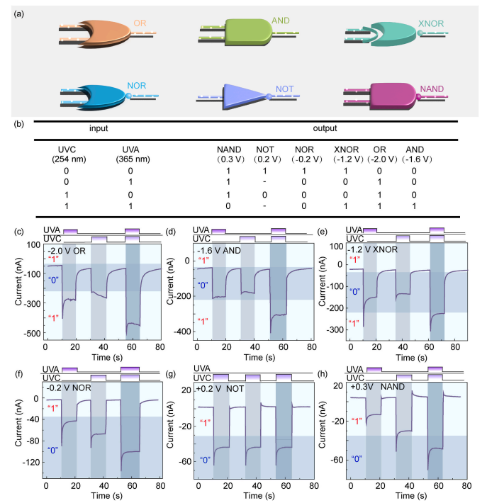
Fig. 6. (a) Schematic diagram of the logic gates. (b) Truth tables of six logic gates. Demonstration of the (c) OR logic gate, (d) AND logic gate, (e) XNOR logic gate, (f) NOR logic gate, (g) NOT logic gate and (h) NAND logic gate.
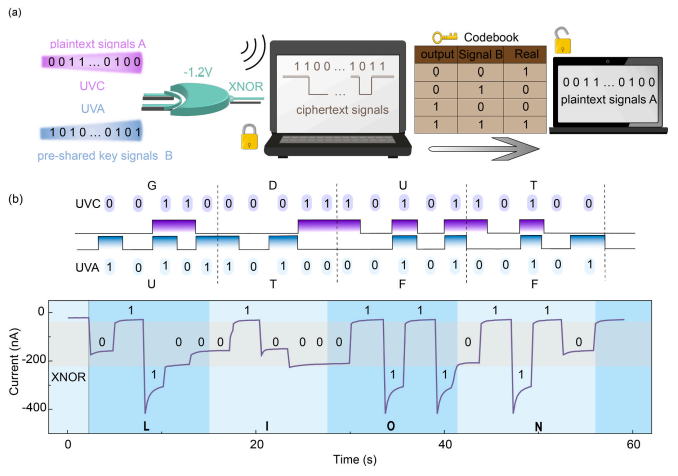
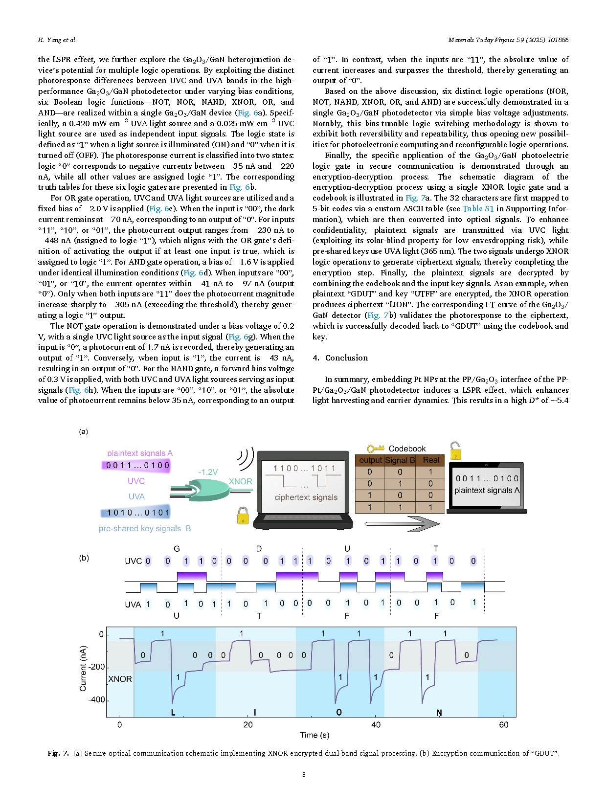
Fig. 7. (a) Secure optical communication schematic implementing XNOR-encrypted dual-band signal processing. (b) Encryption communication of “GDUT”.
DOI:
doi.org/10.1016/j.mtphys.2025.101886