Paper Sharing
【Member Papers】Uniform Wafer-scale MOCVD homoepitaxy of β-Ga₂O₃ on 2-inch (010) substrates
日期:2025-10-31阅读:574
Researchers from the a joint research team from the University of Science and Technology of China, Hangzhou Garen Semiconductor, and the 46th Research Institute of China Electronics Technology Group Corporation have published a dissertation titled "Uniform Wafer-scale MOCVD homoepitaxy of β-Ga2O3 on 2-inch (010) substrates" in Chinese Physics B.
Project Support
This work was supported by the National Natural Science Foundation of China under Grant nos. U23A20358, 62474170, 61925110, 62404214 and 62234007, the University of Science and Technology of China (USTC) Research Funds of the Double First-Class Initiative under Grant No. WK2100000055, the Project of 46th Research Institute of CETC under Grant no. WDZC202446007, the JieBang Headed Project of Changsha City Hunan Province under grant No. kq2301006, and the Opening Project of and the Key Laboratory of Nano devices and Applications in Suzhou Institute of Nano-Tech and Nano-Bionics of CAS. This work was partially carried out at the Center for Micro and Nanoscale Research of USTC. The authors would like to thank Hangzhou Garen Semiconductor Company for providing the casting β-Ga2O3 bulk crystal and MicroAhead from Suzhou for CV test.
Background
Ultrawide bandgap (UWBG) semiconductors have attracted significant attention for next-generation power electronics due to their potential for higher efficiency and power density. Among them, monoclinic β-Ga₂O₃ is particularly promising, offering a theoretical breakdown field of 8 MV/cm and a high Baliga’s figure of merit, surpassing the capabilities of Si, SiC, and GaN. Its anisotropic crystal structure makes the (010) orientation ideal for high-performance lateral devices, but the lack of large-area (010) substrates has historically limited research to small, cleaved samples, hindering scalable device fabrication and wafer-scale uniformity assessment. Advances in melt-growth techniques, such as Czochralski, Vertical Bridgman, EFG, and casting, have recently enabled the production of 2-inch (010) β-Ga₂O₃ wafers, opening the path toward industrial application. Among epitaxial growth methods, metal-organic chemical vapor deposition (MOCVD) is particularly suitable, providing precise control over thickness, doping, and interface quality, making it the key approach for realizing scalable, high-quality epitaxial films on these newly available large-area substrates.
Abstract
The (010) orientation of β-Ga2O3 is a highly promising platform for next-generation lateral power electronics due to its superior theoretical transport properties. However, progress has been impeded by the unavailability of large-area substrates, limiting studies to small-scale samples. Leveraging the recent emergence of 2-inch wafers, we report the first demonstration of homoepitaxial growth on a 2-inch, Fe-doped semi-insulating (010) β-Ga2O3 substrate by metal-organic chemical vapor deposition (MOCVD). A systematic, wafer-scale characterization reveals the successful growth of a high-quality epitaxial film. High-resolution X-ray diffraction shows an excellent crystalline structure, with a rocking curve full-width ranging from 21.0 to 103.0 arcsec. Atomic force microscopy confirms an atomically smooth surface with a root-mean-square roughness below 1.53 nm, displaying a distinct step-flow growth mode across the wafer. Furthermore, mercury-probe capacitance-voltage mapping indicates a well-controlled carrier concentration of ~2×1018 cm-3 with a RSD of 5.12%. This work provides the first comprehensive assessment of 2-inch (010) Ga2O3 epitaxial wafers, validating a critical material platform for the development and future manufacturing of high-performance power devices.
Conclusion
In summary, we have successfully performed the first MOCVD homoepitaxial growth on a 2-inch (010)-oriented β-Ga₂O₃ substrate and conducted the first comprehensive, wafer-scale characterization of the resulting film. Our detailed investigation revealed outstanding material quality across the entire wafer, including an atomically smooth surface with a uniform step-flow morphology (with RMS roughness values between 0.89 nm and 1.53 nm), a superior crystalline structure with XRD rocking curve FWHM ranging from 21.0 to 103 arcsec. Furthermore, we demonstrated precise and uniform control over n-type doping, achieving a carrier concentration of ~2×10¹⁸ cm⁻³ with excellent spatial (RSD≈5.12%) and depth uniformity. This pioneering demonstration not only establishes a robust baseline for device-quality material on a previously unavailable platform but also validates the manufacturability of the (010) β-Ga₂O₃ material system. This work represents a decisive step in advancing lateral Ga₂O₃ power devices from laboratory-scale concepts to a tangible, wafer-level technology poised for commercial impact.
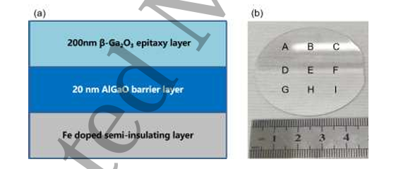
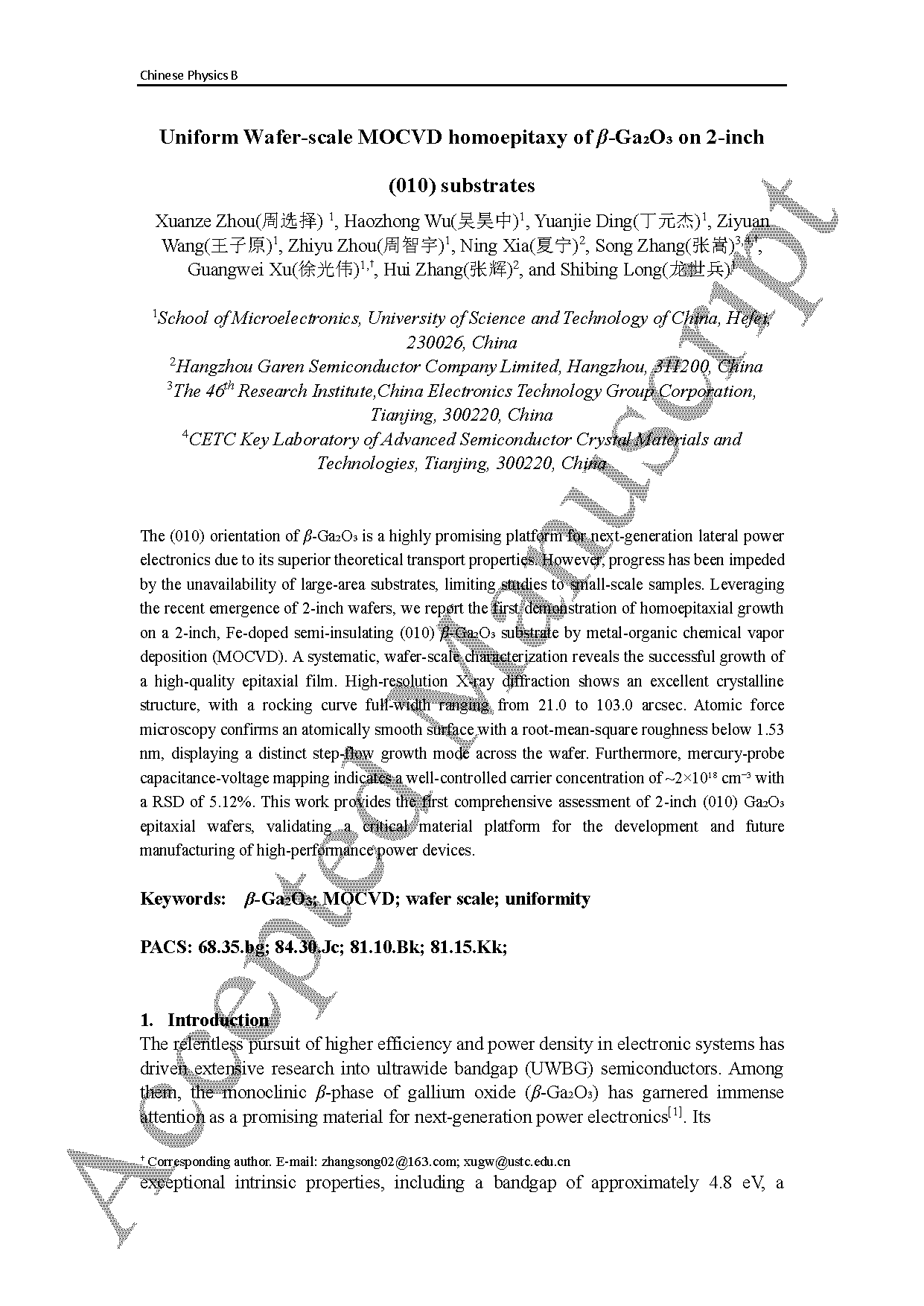
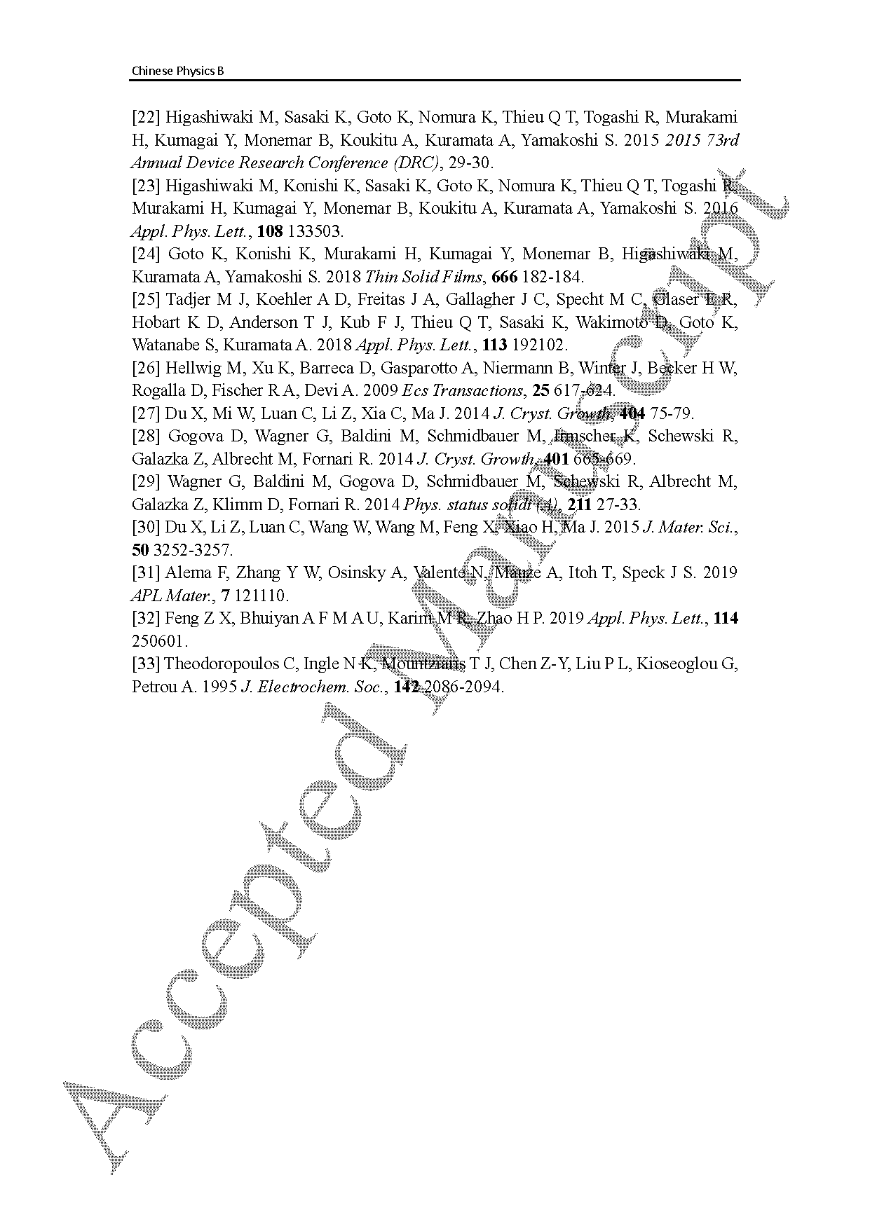
Fig. 1. (a) Schematic diagram of the MOCVD-grown epitaxial structure, consisting of a 200 nm Si-doped Ga₂O₃ channel layer and a 20 nm AlGaO back-barrier on an Fe-doped semi insulating (010) β-Ga₂O₃ substrate. (b) Optical image of the 2-inch wafer illustrating the 9 point mapping locations (A through I) used for systematic characterization.
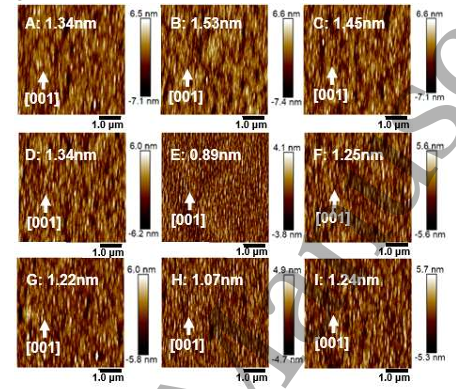
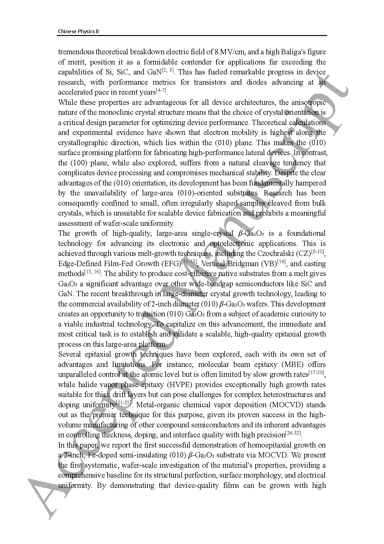
Fig. 2. Surface morphology and summary of structural properties. The 5 µm×5 µm AFM surface morphology scans for the nine designated points (A-I) across the 2-inch wafer all reveal a distinct step-flow growth mode, indicating an atomically smooth surface.
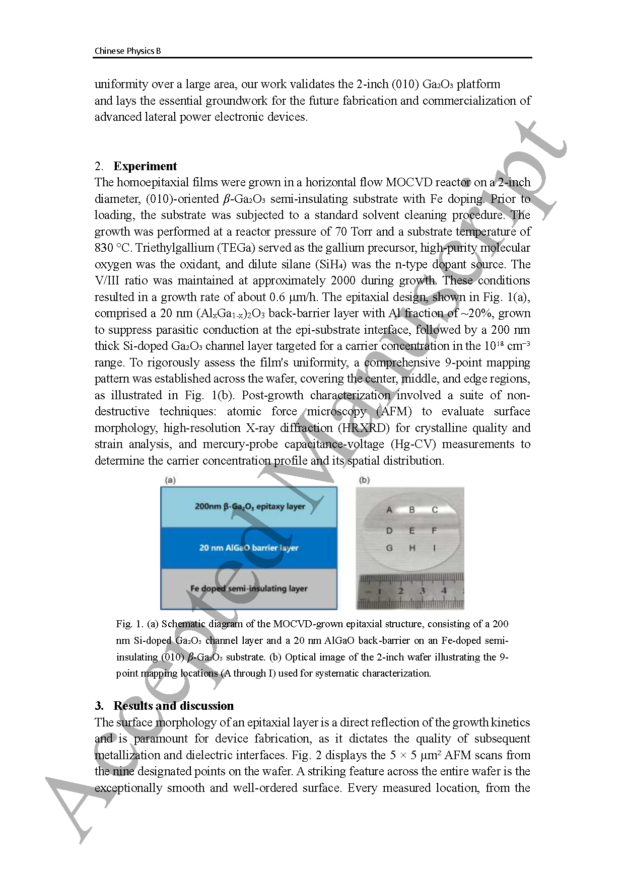
Fig. 3. High-resolution X-ray diffraction rocking curves for the symmetric (020) reflection.
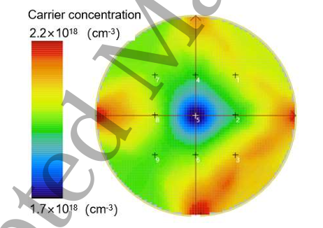
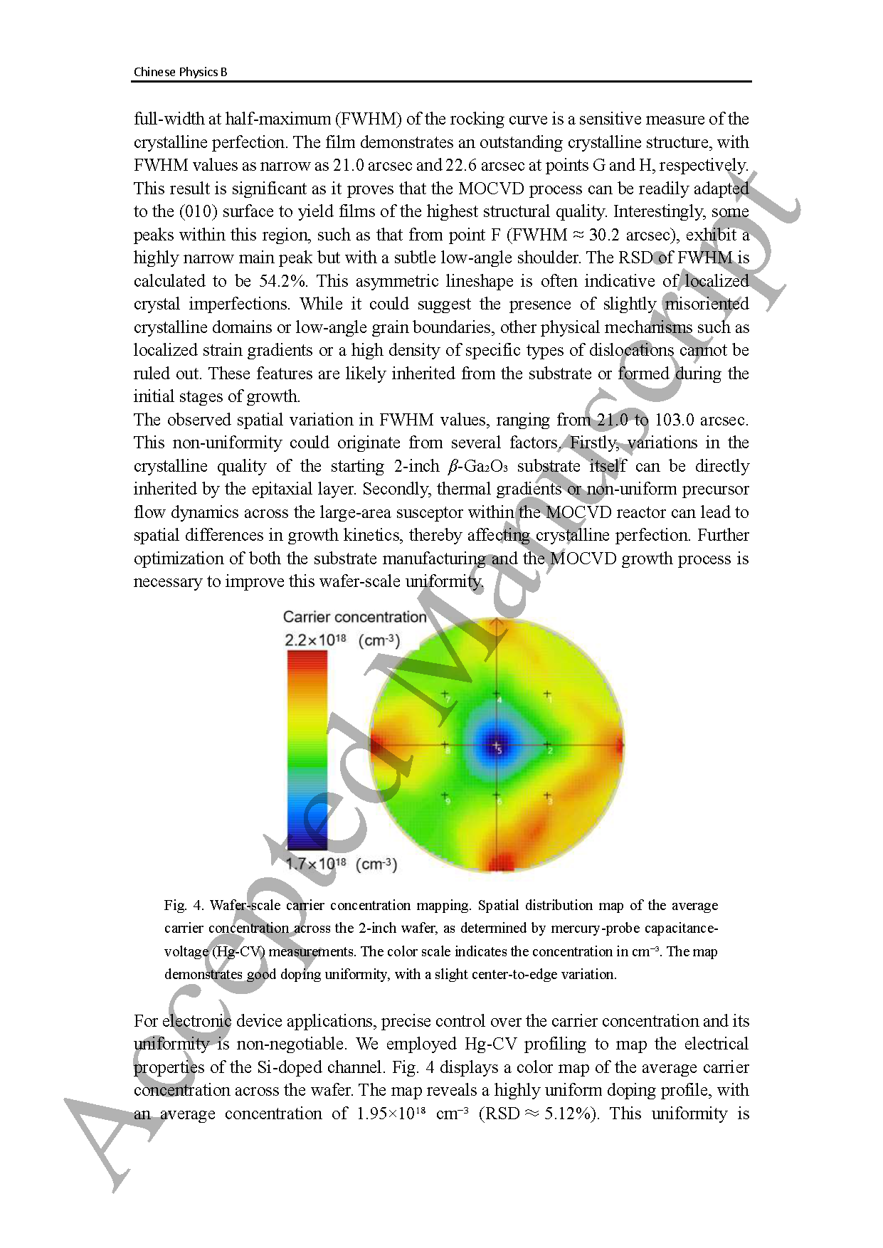
Fig. 4. Wafer-scale carrier concentration mapping. Spatial distribution map of the average carrier concentration across the 2-inch wafer, as determined by mercury-probe capacitance voltage (Hg-CV) measurements. The color scale indicates the concentration in cm⁻³. The map demonstrates good doping uniformity, with a slight center-to-edge variation.
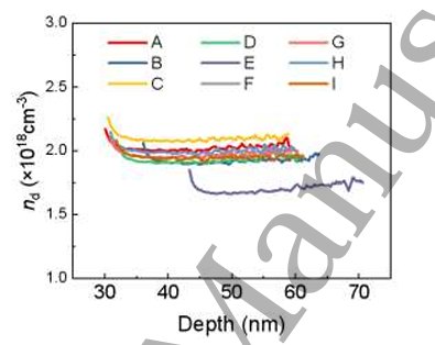
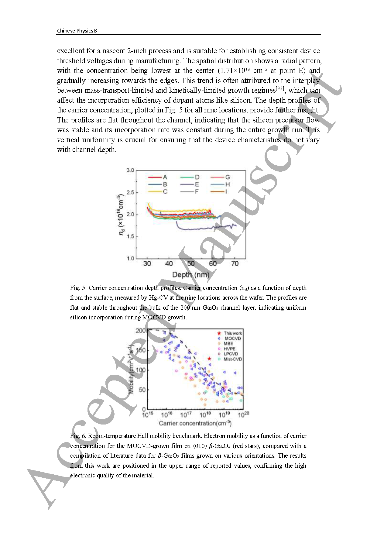
Fig. 5. Carrier concentration depth profiles. Carrier concentration (nd) as a function of depth from the surface, measured by Hg-CV at the nine locations across the wafer. The profiles are flat and stable throughout the bulk of the 200 nm Ga₂O₃ channel layer, indicating uniform silicon incorporation during MOCVD growth.
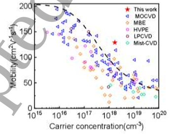
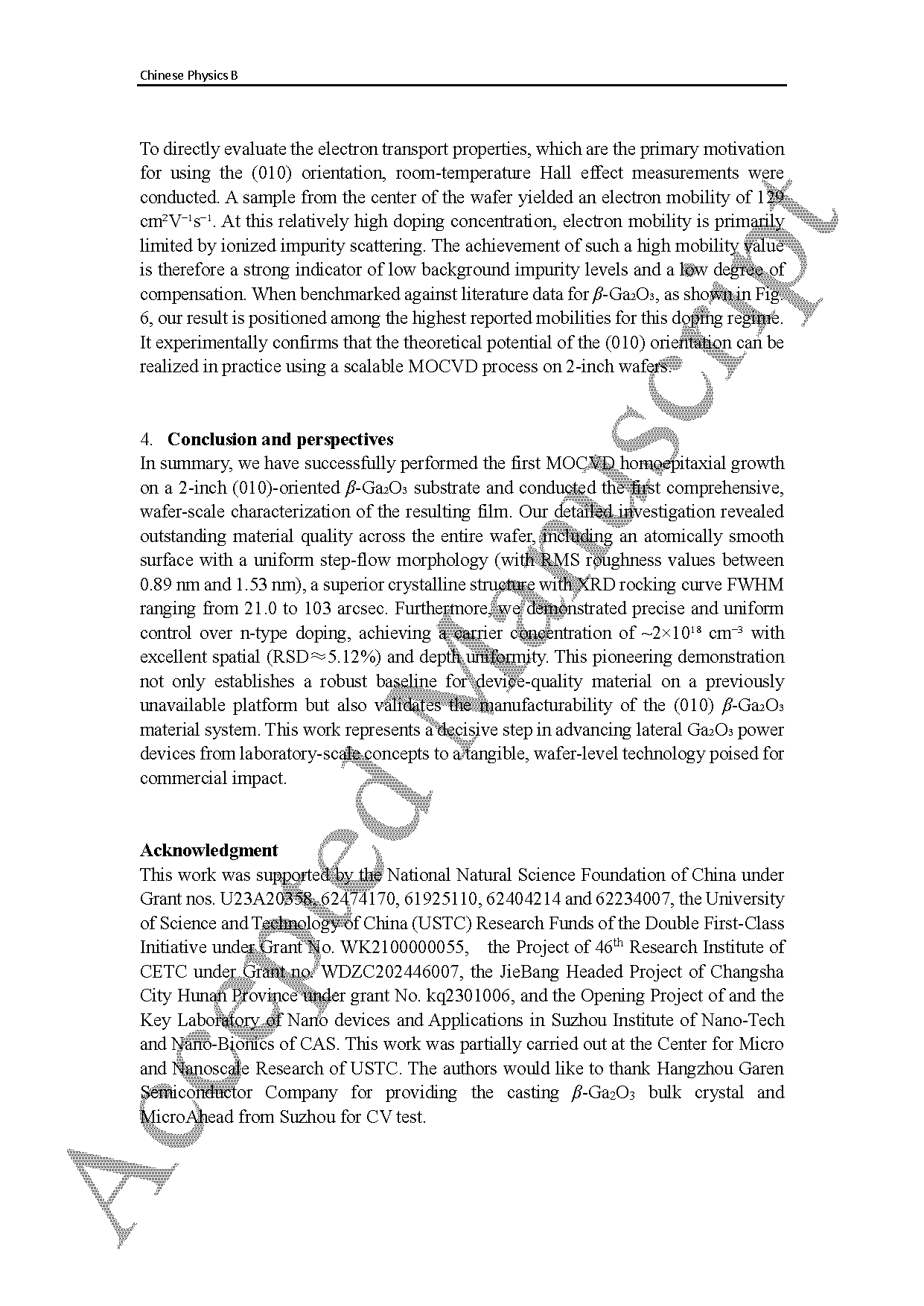
Fig. 6. Room-temperature Hall mobility benchmark. Electron mobility as a function of carrier concentration for the MOCVD-grown film on (010) β-Ga₂O₃ (red stars), compared with a compilation of literature data for β-Ga₂O₃ films grown on various orientations. The results from this work are positioned in the upper range of reported values, confirming the high electronic quality of the material.
DOI:
doi.org/10.1088/1674-1056/ae12e0