Paper Sharing
【Member Papers】Unable phase stabilization optimization for achieving single-phase ε-Ga₂O₃ epitaxy
日期:2025-11-06阅读:752
Researchers from the Xidian University have published a dissertation titled "Unable phase stabilization optimization for achieving single-phase ε-Ga2O3 epitaxy" in Journal of Alloys and Compounds.
Project Support
The work was supported by the General Program of Natural Science Foundation of China (Grant 62274134); The Fundamental Research Funds for the Central Universities (Grant YJSJ24020); National Key Research and Development Program (Grant Nos. 2021YFA0716400 and 2023YFB3609900); The National Science Fund for Distinguished Young Scholars (Grant 61925404); Key R&D Project in Xi’an City (Grant 2023JH-ZCGJ-0013); Aerospace Institute 771 Innovation Fund (Grant 771CX2023007); Interdisciplinary Cultivation Program of Xidian Uni versity (Grant 21103240003).
Background
The research focuses on ε-Ga₂O₃, an ultrawide-bandgap semiconductor characterized by spontaneous polarization and high lattice symmetry. Due to its excellent optical, electrical, and thermal properties, Ga₂O₃ has attracted extensive attention for applications in optoelectronic devices, high-power electronics, and RF resonators. Among its polymorphs (α, β, γ, δ, ε, and κ), ε-Ga₂O₃ stands out for its superior electron mobility and high breakdown voltage. However, obtaining high-quality ε-Ga₂O₃ films remains challenging, as current growth techniques often lead to α–ε mixed-phase films on c-sapphire substrates, hindering device performance improvement.
To address this issue, this study employs a mist chemical vapor deposition (mist-CVD) approach and introduces a tunable phase stabilization optimization strategy. By simultaneously regulating two critical growth parameters—growth temperature and O₂ partial pressure—this method enables controlled transformation from α–ε mixed-phase to phase-pure ε-Ga₂O₃. The approach achieves interface-mediated thermodynamic and kinetic control, promoting ε-phase stabilization while suppressing secondary phase formation. As a result, high-quality, atomically smooth, single-phase ε-Ga₂O₃ films with coherent ε (002) orientation are obtained. This work provides new insights into phase stabilization mechanisms in Ga₂O₃ epitaxy.
Abstract
ε-phase gallium oxide (ε-Ga2O3), with its inherent spontaneous polarization and high lattice symmetry, is a promising candidate for ultrawide bandgap electronics and piezoelectric devices. However, achieving phase-pure ε-Ga2O3 remains a significant challenge due to competing nucleation pathways and polycrystalline orientation competition, often leading to mixed-phase formation and structural defects. In this study, we report a tunable phase stabilization optimization tailored for mist chemical vapor deposition (mist-CVD), involving the simultaneous control of growth temperature and O2 partial pressure to finely modulate growth thermodynamics and kinetics. This approach effectively suppresses disordered phase orientations and promotes a controlled transition from α–ε mixed phases to a high-purity single ε-phase. The resulting ε-Ga2O3 films on c-sapphire exhibit a full width at half maximum (FWHM) of 0.073° and a root-mean-square (RMS) roughness of 0.75 nm, indicating high crystallinity and surface smoothness. High-resolution transmission electron microscopy (HRTEM) reveals a clear polycrystalline-to-epitaxial transition layer and confirms a coherent ε (002) out-of-plane orientation. Importantly, the application of this approach to surface acoustic wave (SAW) devices yields a center frequency of 1.69 GHz and an effective coupling coefficient (keff2) of 0.328 %, demonstrating the functional viability of the obtained films. This work establishes a reproducible and interface-sensitive pathway for ε-Ga2O3 epitaxy and underscores the importance of interface engineering and phase control strategies in enabling the practical deployment of ultrawide bandgap oxide semiconductors.
Highlights
● Phase-pure ε-Ga2O3films grown on c-sapphire by mist-CVD via interface-mediated control.
● Growth temperature and O2pressure optimization enables selective ε-phase formation.
● Polycrystalline orientation competition guides ε/α transition via interfacial matching.
● Record FWHM 0.073°, RMS 0.75 nm, and 1.69 GHz SAW device performance achieved.
● Phase stabilization optimization unlocks new potential in ultrawide bandgap oxides.
Conclusion
In this study, we identified a distinct polycrystalline orientation competition layer at the early stage of ε-Ga2O3 film growth, whose evolution is strongly influenced by growth temperature and O2 partial pressure. By systematically tuning these parameters, we developed a phase stabilization optimization mediated by the film/substrate inter face, which modulates both thermodynamic and kinetic factors governing phase formation. Specifically, the interface between c-sapphire and Ga2O3 introduces a lattice mismatch and interfacial energy landscape that initially leads to mixed-phase nucleation. However, as the growth temperature increases to 620 ℃, the release of interfacial strain energy and improved lattice matching facilitate a transition from the α–ε mixed-phase to a single ε-phase. Concurrently, a higher O2 partial pressure slows down the growth rate, yielding thinner poly crystalline transition layers and promoting vertical grain alignment. Together, these interface-governed effects suppress random Ga atom migration, reduce phase disorder, and enable selective stabilization of ε-Ga2O3. As a result, the obtained ε-Ga2O3 films exhibited a significantly reduced full width at half maximum (FWHM) of 0.073◦, surpassing the MOCVD benchmark value of 0.09◦, along with a root-mean-square surface roughness of just 0.75nm. These improvements demonstrate the capability of our approach to simultaneously enhance phase purity and surface morphology. Furthermore, surface acoustic wave (SAW) devices were successfully fabricated using the ε-Ga2O3 films as piezoelectric layers, achieving a resonant frequency of 1.69GHz and an effective electromechanical coupling coefficient (keff2) of 0.328%. These results validate the potential of our interface engineering- based phase stabilization optimization for enabling high-quality ε-Ga2O3 epitaxy and demonstrate its relevance for next-generation ultrawide bandgap electronic and piezoelectric applications.
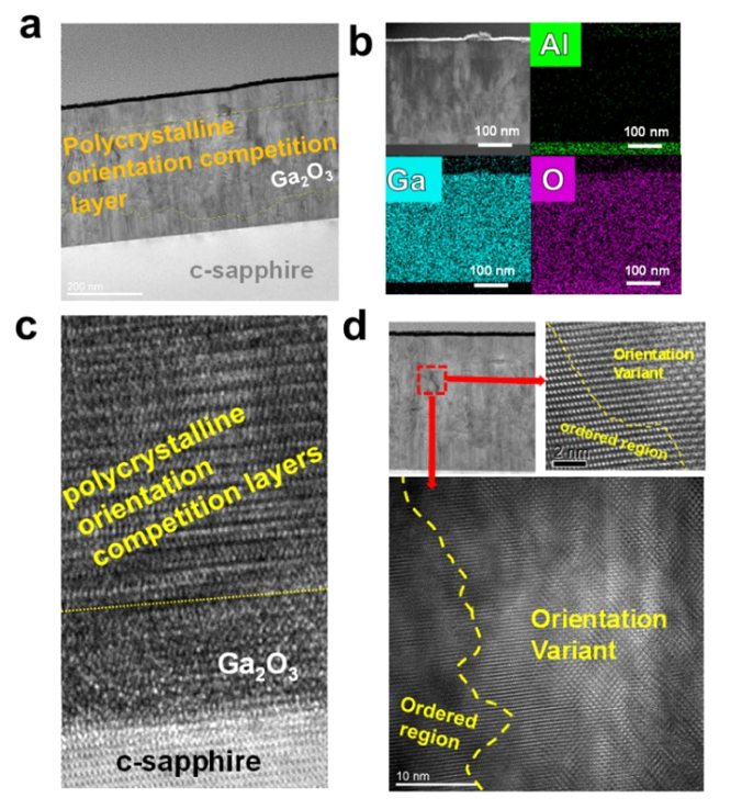
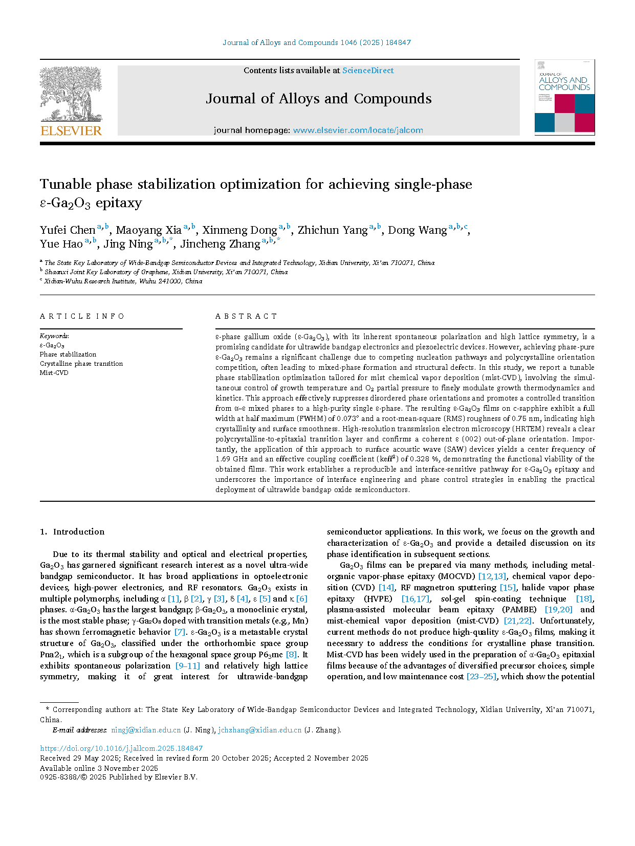
Fig. 1. Microstructure of Ga2O3 films with different phases. (a) HAADF STEM imaging of the FIB cross-section sample. (b) STEM–EDX elemental mapping at the c- sapphire/ Ga2O3 interface. (c) HRTEM image of the c-sapphire/Ga2O3 interface. (d) HAADF of the phase-conversion region of Ga2O3 (red dashed box); the bottom image corresponds to the HRTEM amplification of the converted phase.

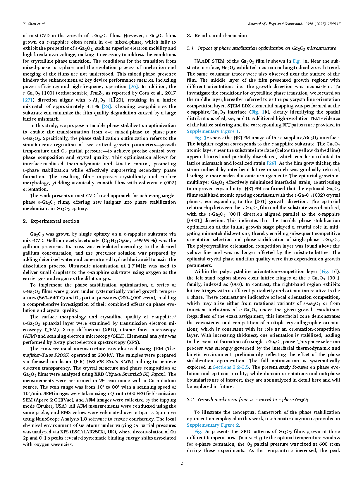
Fig. 2. Structural and Morphological Characterization of Ga2O3 Films Grown at Different Temperatures. (a) XRD of Ga2O3 films at 560℃, 620℃, and 640℃. (b) FWHM line diagram of the XRD of Ga2O3 films at different growth temperatures. (c) Y-error plot of the RMS surface roughness for Ga2O3 films grown at 560℃-640℃. (d) SEM surface topography of Ga2O3 film at 620℃. AFM surface topography of the Ga2O3 films on the c-sapphire substrate at (e) 560℃, (f) 620℃, and (g) 640℃.
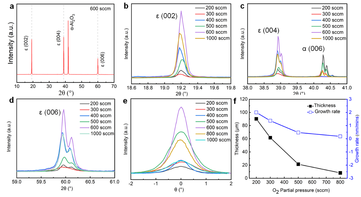
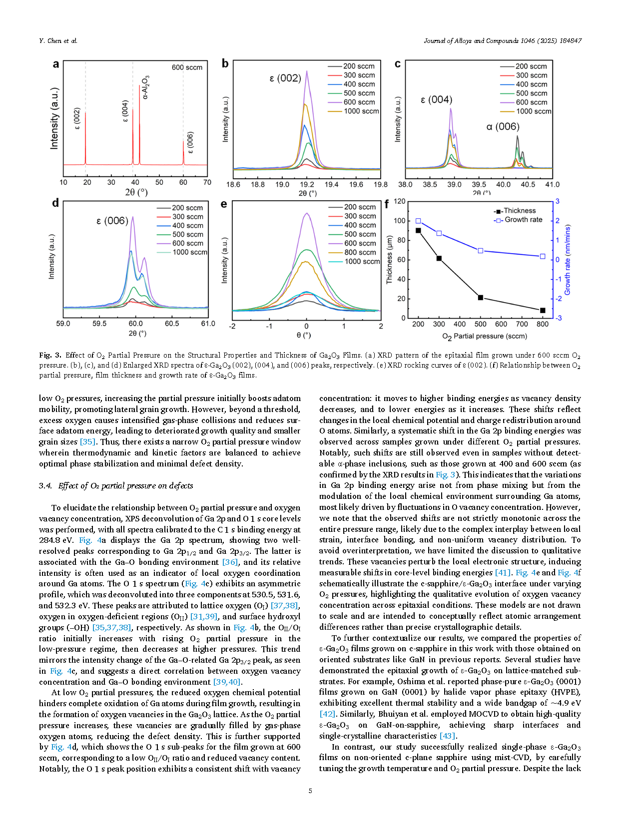
Fig. 3. Effect of O2 Partial Pressure on the Structural Properties and Thickness of Ga2O3 Films. (a) XRD pattern of the epitaxial film grown under 600 sccm O2 pressure. (b), (c), and (d) Enlarged XRD spectra of ε-Ga2O3 (002), (004), and (006) peaks, respectively. (e) XRD rocking curves of ε (002). (f) Relationship between O2 partial pressure, film thickness and growth rate of ε-Ga2O3 films.
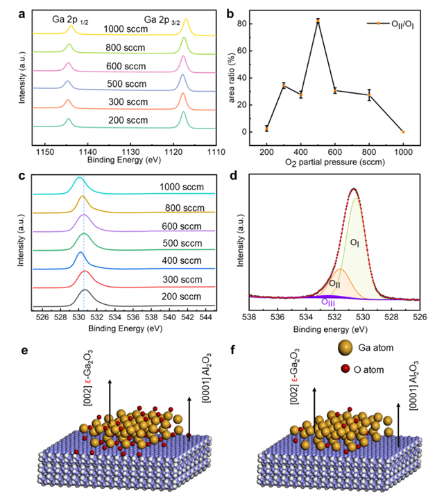
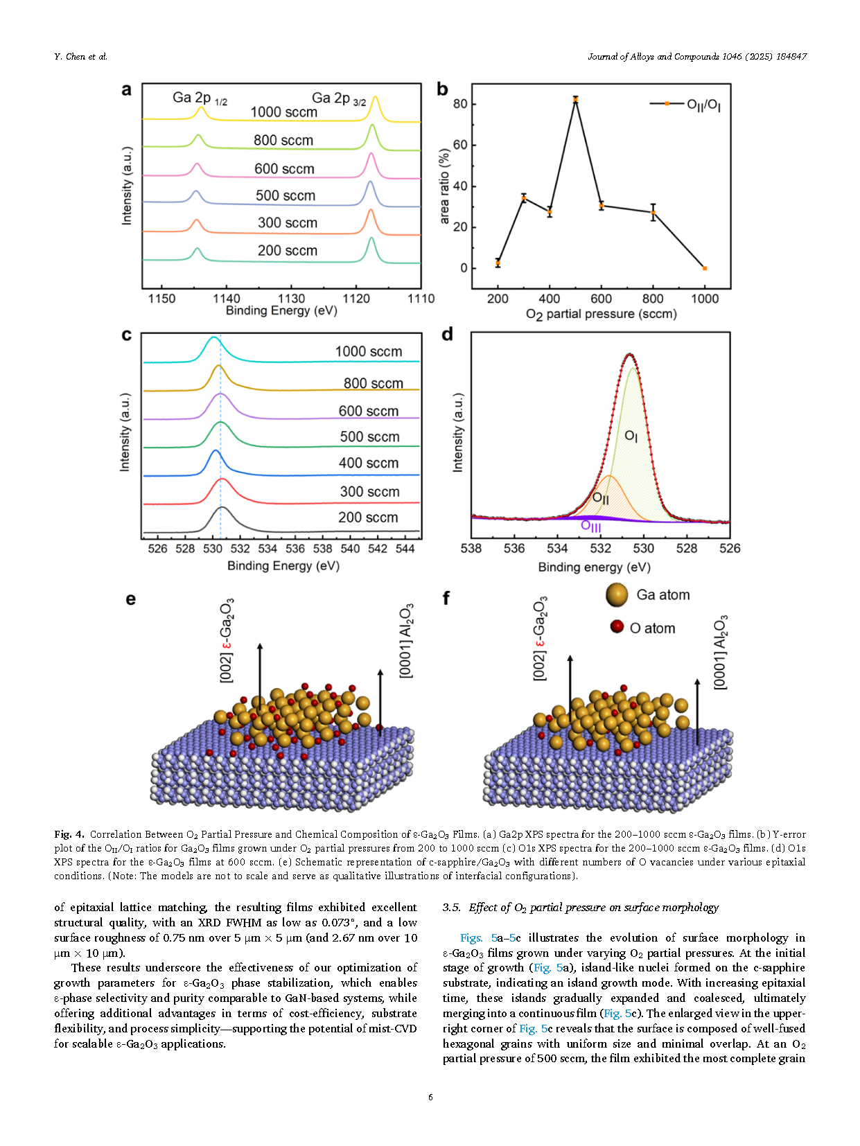
Fig. 4. Correlation Between O2 Partial Pressure and Chemical Composition of ε-Ga2O3 films. (a) Ga2p XPS spectra for the 200–1000 sccm ε-Ga2O3 films. (b) Y-error plot of the OII /OI ratios for Ga2O3 films grown under O2 patrial pressures from 200 to 1000 sccm (c) O1s XPS spectra for the 200–1000 sccm ε-Ga2O3 films. (d) O1s with different numbers of O vacancies under various epitaxial conditions. (Note: The models are not to scale and serve as qualitative illustrations of interfacial configurations).
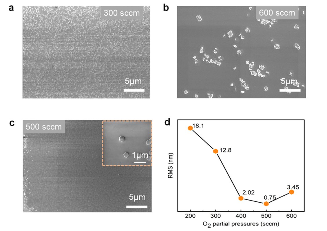
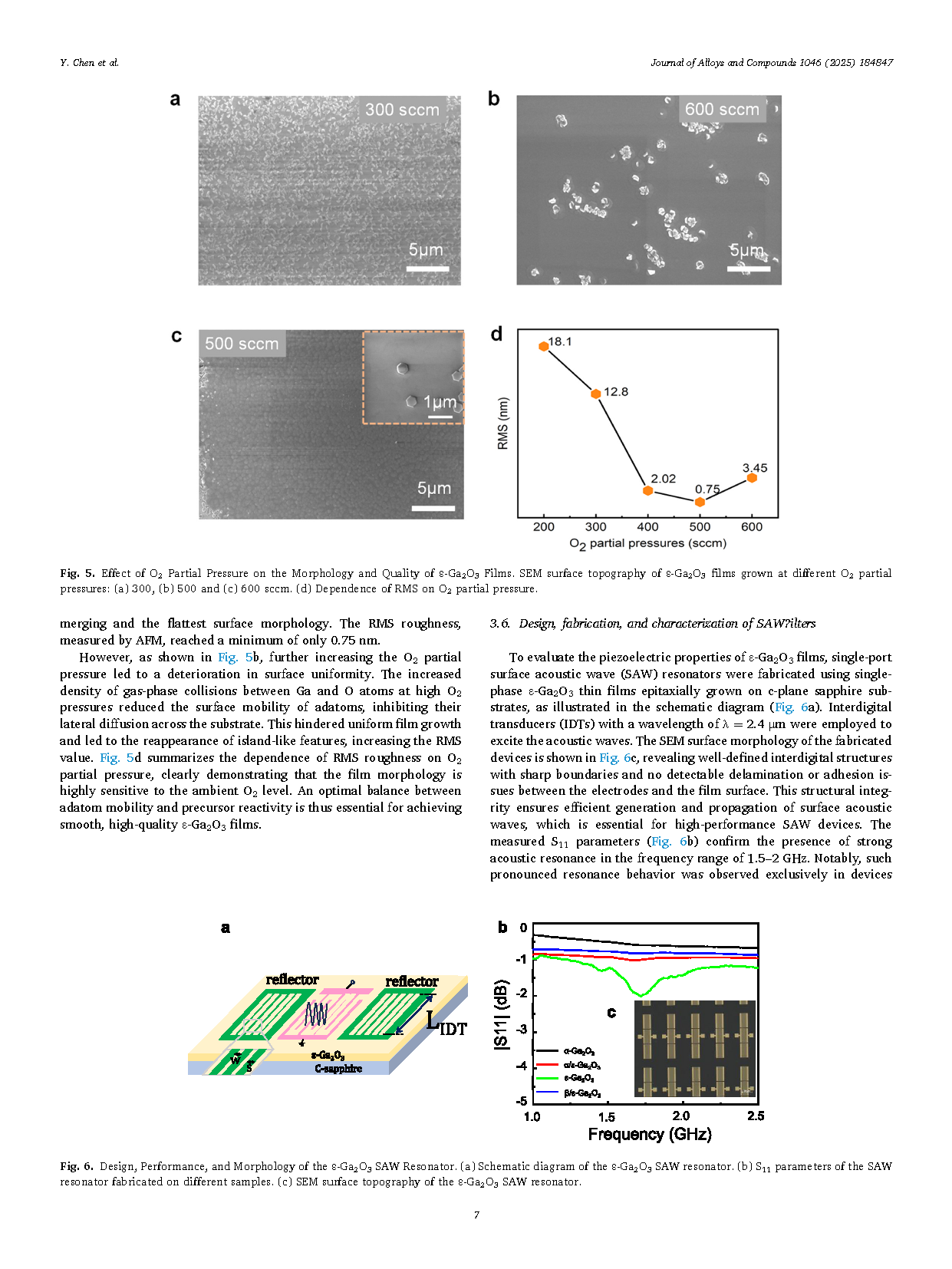
Fig. 5. Effect of O2 Partial Pressure on the Morphology and Quality of ε-Ga2O3 Films. SEM surface topography of ε-Ga2O3 Films grown at different O2 partial pressures: (a) 300, (b) 500 and (c) 600 sccm. (d) Dependence of RMS on O2 Partial Pressure.
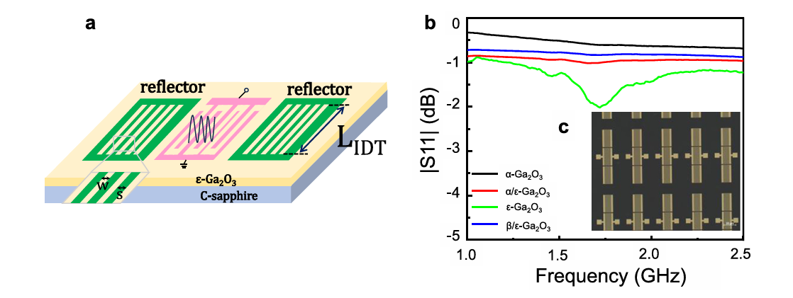
Fig. 6. Design, Performance, and Morphology of the ε-Ga2O3 SAW Resonator. (a) Schematic diagram of the ε-Ga2O3 SAW resonator. (b) S11 parameters of the SAW resonator fabricated on different samples. (c) SEM surface topography of the ε-Ga2O3 SAW resonator.
DOI:
doi.org/10.1016/j.jallcom.2025.184847