Member Intro
【Member Intro】Suzhou Raphael Optech Co., Ltd.—— Regular Member
日期:2025-11-11阅读:1106
I. Company Profile

Suzhou Raphael Optech Co., Ltd. is a high-tech enterprise specializing in the research, development, and manufacturing of advanced optical inspection and imaging systems. The company was registered in August 2018 in Taicang, Suzhou, with an R&D center and branch office in Shanghai, and a liaison office in Shenzhen.
Raphael boasts a research team led by PhDs from prestigious universities including Tsinghua University, Soochow University, and University of Shanghai for Science and Technology. To date, the company has been granted more than 50 invention and utility model patents, along with 10 software copyrights.
The company is also a member of the National Technical Committee for Standardization of Optics and Photonics and the Microscope Subcommittee under the same national standards body.
Raphael’s product portfolio includes freeform 3D surface measurement instruments, wafer warpage and thin-film stress measurement systems, 3D measurement microscopes, internal stress detectors, ultra-deep-field microscopes, and precision optical lenses. These products are widely applied in precision optics manufacturing, semiconductor wafers, smart automotive electronics, smart device displays, AR/VR products, and other high-end manufacturing lines. The company’s technologies are domestically leading and have achieved mass production capabilities.
Suzhou Raphael Optech Co., Ltd. aims to become a leading provider of 3D inspection equipment, offering precise “eyes” for advanced manufacturing. Guided by a strategy of safeguarding high-end intelligent manufacturing, the company’s mission is to enhance customers’ inspection efficiency and product quality. By combining professional technical services with in-depth understanding of clients’ operations, Raphael provides comprehensive 3D inspection solutions from R&D to production and quality control.
Facing the industrial wave of fourth-generation semiconductors represented by Gallium Oxide (Ga₂O₃), Raphael has proactively deployed core inspection technologies, focusing on key challenges such as microscopic morphology, stress distribution, and defect identification, driving the intelligent upgrade of the wide-bandgap semiconductor industry.
As an ultra-wide bandgap semiconductor, Ga₂O₃ offers high breakdown field strength (4.8 eV), excellent thermal stability, and low-cost fabrication, showing tremendous potential in high-power electronics, solar-blind UV detectors, and energy-efficient power grids. However, microscopic defects generated during production can significantly reduce device performance and yield. Traditional inspection methods suffer from low efficiency, sample damage, and difficulty in real-time monitoring.
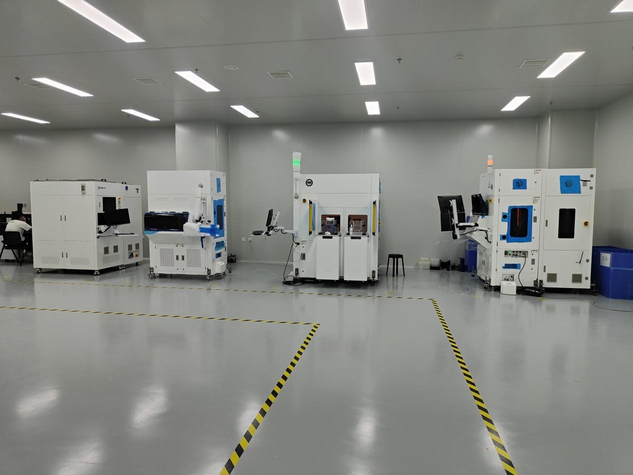
Raphael Optech, with the mission of “Meticulous Attention, Pursuit of Excellence,” focuses on Ga₂O₃ wafer inspection and has independently developed a series of industry-leading inspection technologies and equipment. The company offers a full range of inspection devices for both laboratory (semi-automatic) and mass production (fully automatic) environments, meeting diverse application scenarios. By improving product yield through precise inspection, Ruifei significantly reduces downstream manufacturing costs, enhances inspection efficiency, and shortens product development cycles.
The company continues to invest in innovative inspection technologies for Ga₂O₃ and other wide-bandgap semiconductors, aiming to become a global leader in high-end semiconductor inspection equipment. By building an integrated development model of technology R&D, standard setting, and industry services, Raphael Optech strives to give China a competitive edge in the fourth-generation semiconductor market and contribute to global semiconductor innovation.
II. Products:
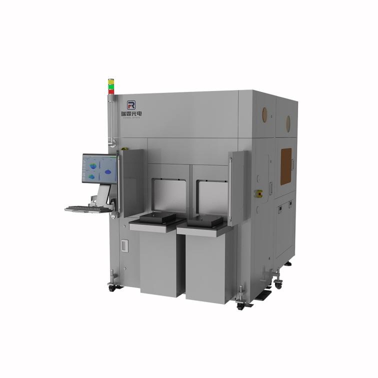
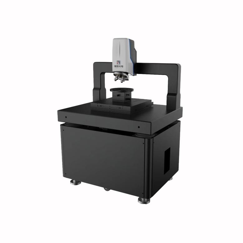
● Product 1: Fully Automatic Geometric Surface Measurement System
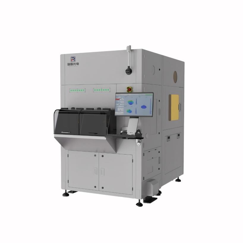
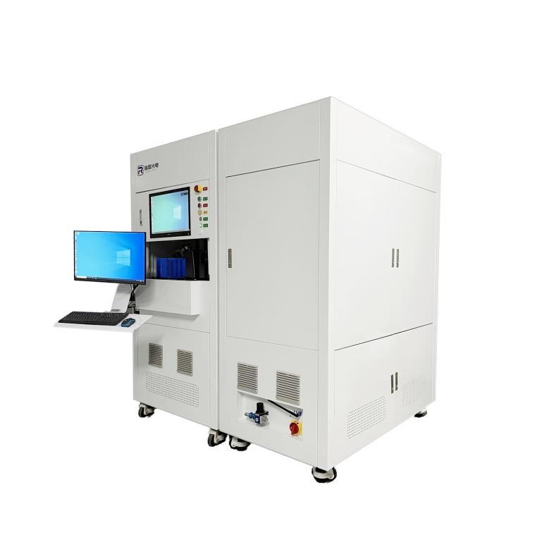
● Product 2: Fully Automatic Wafer Warpage and Thin-Film Stress Measurement System
● Product 3: Multi-Mode 3D Measurement Microscope
● Product 4: Fully Automatic Wafer Internal Stress Detector
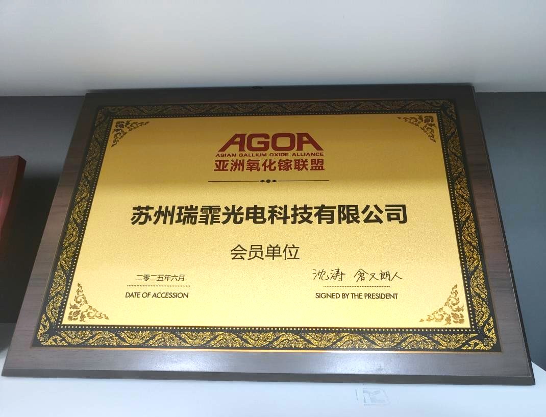
III.Photo of the Member's Plaque