Conference News
【Conference Information】APCSCRM 2025 Preview: The Alliance Guides You Through the Key Highlights of Gallium Oxide
日期:2025-11-23阅读:1015
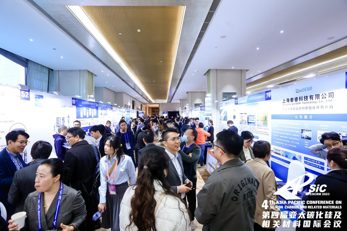
The 6th Asia-Pacific Conference on Silicon Carbide and Related Materials (APCSCRM 2025) will be grandly held in Zhengzhou, Henan, from November 25 to 27, 2025. Centered on the theme “Wide Bandgap, Wider Future,” the conference will focus on innovation across the entire wide-bandgap semiconductor value chain, covering key technological segments such as equipment, materials, devices, packaging and testing, as well as end applications. It will explore in depth the industrialization prospects of wide-bandgap technologies in power electronics, renewable energy, communications, intelligent transportation, and other critical fields.
As a major international platform for academic and industrial exchange in the wide-bandgap semiconductor community, the Asia-Pacific Conference on Silicon Carbide and Related Materials (APCSCRM) has been successfully held five times since its inaugural meeting in Beijing in 2018. The conference has attracted nearly 4,000 distinguished participants from more than ten countries and regions including China, Europe, the United States, Japan, and South Korea, bringing together over 1,000 enterprises and presenting more than 300 technical reports. After years of development, APCSCRM has become one of the most influential professional forums in the Asia-Pacific region, recognized for both its industrial depth and academic excellence.
As a strategic partner of the Innovation Association of Wide Bandgap Semiconductor Technology, the Asian Gallium Oxide Alliance will take an active role in this year’s conference and will host an exhibition booth (Booth No. 91). In the upcoming updates, the Alliance will highlight Gallium Oxide-related topics, offering a curated overview of noteworthy presentations and key achievements from our member organizations—providing a comprehensive, multi-dimensional perspective on the core technical focuses of the conference.
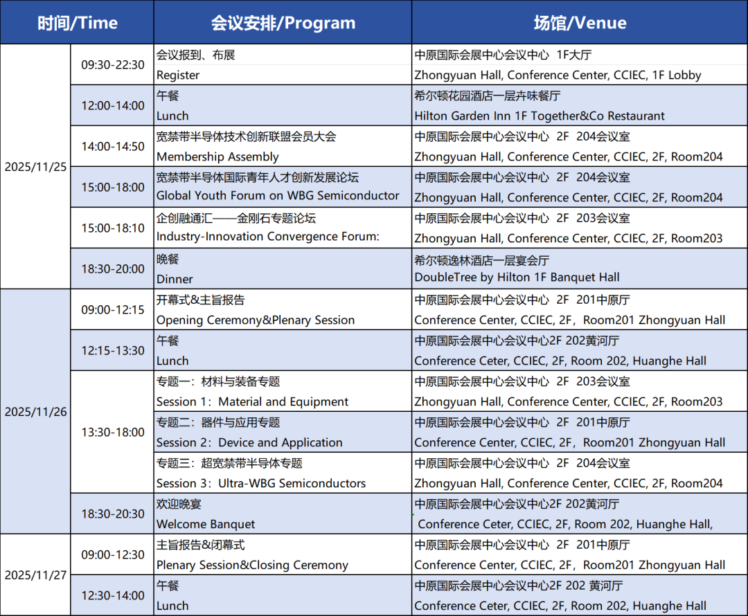
Meeting Schedule Overview
Conference Schedule
Presentations Related to Ga₂O₃
In the 6th Asia-Pacific Conference on Silicon Carbide and Related Materials (APCSCRM 2025), the topic of gallium oxide will also receive significant attention. Experts and scholars from leading domestic and international research teams will deliver presentations covering Ga₂O₃ epitaxy, growth mechanisms, device physics, and cutting-edge applications, showcasing the latest progress and key breakthroughs in current Ga₂O₃ research. A summary of the related reports is provided below.
Global Youth Forum on WBG Semiconductor >> 11/25 17:45-18:25
First-Principles Study on β-GeS2/β-Ga2O3 :Heterojunction
LlU Huan, Inner Mongolia University of Technology
Plenary Session >> 11/26 10:15-10:30
Bridging the Gap from Gallium Oxide Research to Industrialization: From Existence toPractical Application
Ql Hongji, Hangzhou Fujia Gallium Technology Co.,Ltd., Chairman
Plenary Session >> 11/27 09:00-09:25
Ultra-wide bandgap semiconductor gallium oxide and gallium-based spinel crystals
TAO Xutang, Shandong University, Professor
Session 3:Ultra-WBG Semiconductors >> 11/26 13:30-13:50
Gallium Oxide-Based Solar-blind Ultraviolet Photonic Devices and Applications
TANG Weihua, Ga0 Semi, Chairman
Session 3:Ultra-WBG Semiconductors >> 11/26 13:50-14:10
Ultra-wide bandgap gallium oxide for next generation high-power electronics:growth, doping and defects study
Daniela Gogova, Linköping University, Principal Research Engineer
Session 3:Ultra-WBG Semiconductors >> 11/26 14:10-14:30
Progress in Gallium Oxide Thin Film Epitaxy and doping
Tan Chee Keong, Tanoxi Technology, CEO, The Hong Kong University of Science and Technology (Guangzhou),Assistant Professor
Session 3:Ultra-WBG Semiconductors >> 11/26 14:30-14:50
O2 sensors for λ-probe and high-temperature CH4 sensors based on β-Ga2O3 microcrystals and thin film structures
Aleksei Almaev, Tomsk State University, Head of the laboratory
Member Exhibitors
A total of 10 Alliance member companies are participating in this conference, covering areas such as materials, growth equipment, epitaxy, and devices. They collectively showcase the latest achievements and technological layouts across the entire Ga₂O₃ industry chain. Next, the Alliance will guide you through the relevant information regarding these member companies.
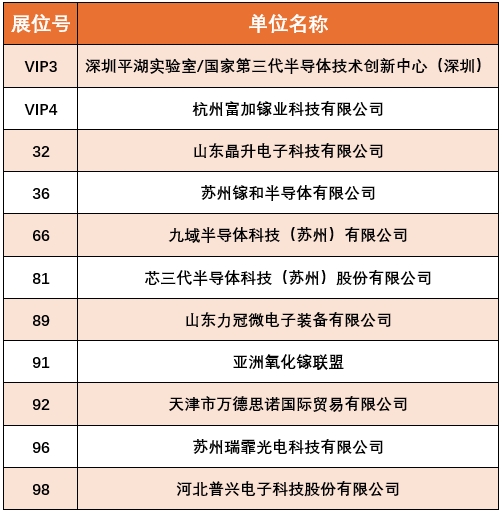
BOOTH:VIP3
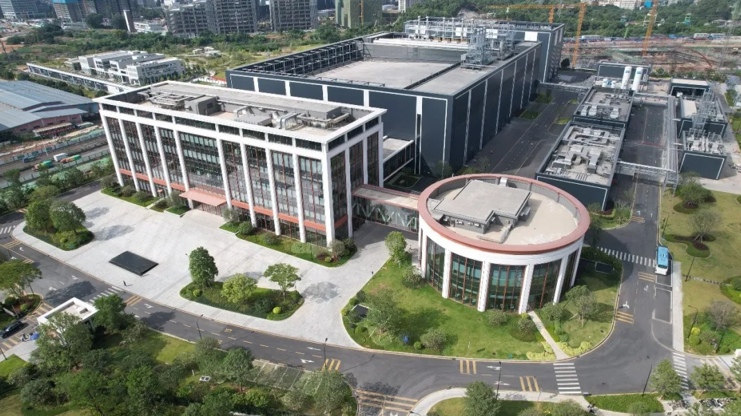
National Center of Technology Innovation for Wide Bandgap Semiconductor (Shenzhen) was awarded by the Ministry of Science and Technology in December 2021 and held by Shenzhen Municipal Science, Technology and Innovation Commission in August 2022. Shenzhen Pinghu Laboratory was established as the main operating unit, focusing on SiC and GaN and the next generation of advanced power electronic materials and devices, core equipment and parts, supporting materials and other fields. To carry out core technology research.
The laboratory is located in Luoshan Science and Technology Park, Longgang District, Shenzhen, covering an area of 130 mu, 100 class clean room area of 9500 square meters, with industry-leading wide band gap power semiconductor infrastructure, more than 380 sets of international and domestic advanced equipment. The laboratory has a manpower of over 390 people, bringing together top talents at domestic and international to build an open, public and shared scientific research, pilot test and analysis platform for the whole country, and jointly build a sustainable future.
BOOTH:VIP4
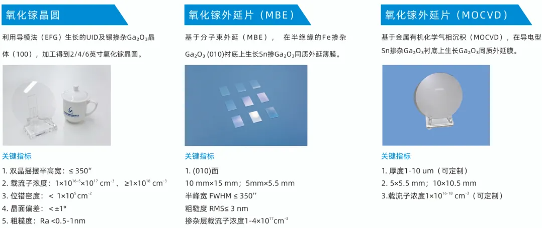
Hangzhou Fujia Gallium Technology Co., LTD., founded on December 31, 2019, is the first "hard technology" enterprise registered by Hangzhou Institute of Optics and Fine Mechanics. With the vision of "Making the World Use Good Materials", the company focuses on the industrialization work of wide bandgap semiconductor Gallium Oxide materials. The core products include Gallium Oxide single crystal substrates, MOCVD epitaxial wafers, MBE epitaxial wafers, The VB method and EFG method crystal growth equipment, substrate grinding and polishing equipment, etc. provide systematic solutions for material development, accelerate the full chain connection of the ultra-wide bandgap Gallium Oxide industry, and promote the application of Gallium Oxide materials in power devices, microwave and radio frequency devices, and optoelectronic detection fields.The company's series of important achievements in the development of Gallium Oxide have been featured and reported by well-known media such as People's Daily, Xinhuanet, China Securities News, and The Paper.

BOOTH:32
Shandong Jingsheng Electronic Technology Co., Ltd. is a national-level high-tech enterprise focusing on the research and development and production of semiconductor equipment. The company's main products are the third and fourth generation semiconductor high-end equipment and a variety of crystal growth equipment, which are widely used in integrated circuit power devices, semiconductor materials, solar cells, LED chip manufacturing, new energy and other fields.
Jingsheng Electronics pays attention to technological innovation, owns a number of independent intellectual property rights, and is committed to providing customers with high quality products and solutions. Adhering to the business philosophy of "integrity, innovation, cooperation and win-win", the company continues to improve its core competitiveness and promote the technological progress of the industry.

BOOTH:36
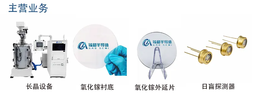
Suzhou GAO Semiconductor Co., Ltd. is a high-tech enterprise specializing in ultra-wide bandgap semiconductor materials—gallium oxide (Ga2O3). Committed to overcoming key technological barriers in the Ga2O3 industry, the company integrates material R&D, device design, and production applications. It is dedicated to providing high-performance Ga2O3 materials and solutions to drive innovation in next-generation power electronics. Currently, the company has successfully mastered 6-inch Ga2O3 crystal growth technology, achieving stable mass production of high-quality single-crystal substrates. The company offers a range of highly customized material, epitaxial, and device development services, closely aligning with customers' early-stage R&D needs to drive technological breakthroughs and product innovation.
BOOTH:66
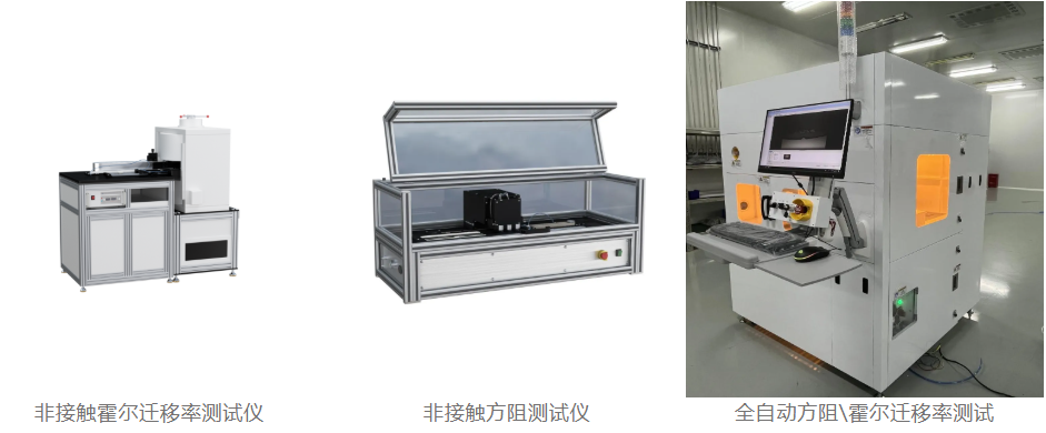
Founded in 2021, the company is a manufacturer of contactless semiconductor testing and analysis equipment with world-leading technology, registered in Suzhou. The company integrates research and development, design, manufacturing and sales, mainly overcoming foreign monopoly technology, replacing imported products, and making semiconductor material testing equipment domestic.
The main products: Non-contact nondestructive square resistance tester, wafer sheet resistance tester, sheet resistance tester, silicon resistivity tester, high and low resistivity analyzer eddy current method, bulk crystal resistivity analyzer, eddy current resistivity probe and PN probe tester, the migration rate (hall) tester, minority carrier lifetime tester, wafer and silicon wafer thickness tester, surface photovoltage JPV \ SPV. And provide testing and solutions for Silicon Carbide, silicon wafers, Gallium Nitride, Gallium Oxide, metal films, glass, substrates and epitaxy manufacturers.
With advanced technology and rich product lines, it has developed into one of the few semiconductor special equipment suppliers in Chinese Mainland with certain international competitiveness. Its products have been recognized by many mainstream semiconductor manufacturers at home and abroad, and have won good market reputation.
BOOTH:81
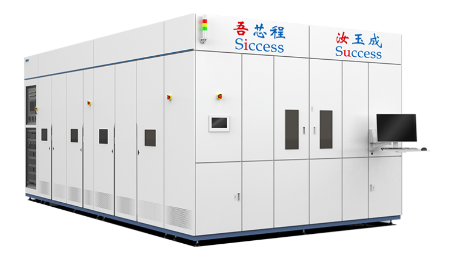
Founded in 2020 in Suzhou Industrial Park, SiCentury is a cutting-edge semiconductor manufacturing equipment provider with world-class talents and independent intellectual property rights. With a global vision, SiCentury is committed to establishing the world’s leading platform for key equipment and core technology in semiconductor industry. Our core management and technical experts boast decades of successful experience in R&D and commercialization of high-end semiconductor manufacturing equipment.
SiCentury focuses on R&D, manufacturing, sales, and service of SiC/GaN and other compound semiconductor epitaxy equipment, providing global customers with world-class equipment and advanced technological solutions tailored for mass production and prospective research. Going forward, we plan to expand our portfolio to a wide range of semiconductor equipment.
SiCentury was the first manufacturer in China to realize volume sales of 6” and 8” silicon carbide epitaxy equipment with vertical gas flow, which has continued to be used by more than a dozen top industry customers for mass production.
BOOTH:89
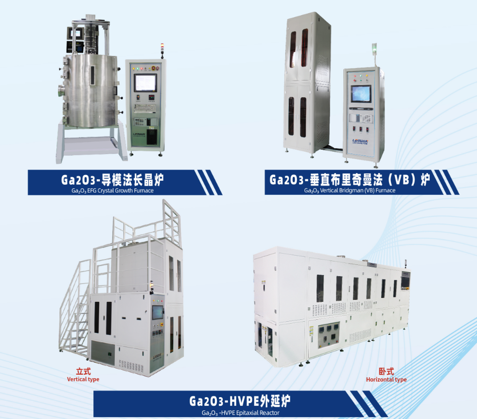
Shandong Liguan Microelectronics Equipment Co., LTD. (abbreviation: Shandong Liguan), founded in 2013. After 12 years of development, Shandong Liguan has become a domestic and foreign advanced semiconductor equipment manufacturing and process technology service provider integrating R&D, production and sales.
The company's products cover the first generation to the fourth generation of semiconductor material process equipment, all with independent intellectual property rights, completely independent and controllable, products are widely used in integrated circuits, power semiconductors, compound semiconductors, 5G chips, optical communication, MEMS and other new electronic device manufacturing fields.
The company can provide customers with an integrated solution of "equipment manufacturing + process technical service".
The company always firmly believes in the scientific development concept of "scientific and technological innovation is the first productive force", adheres to innovation-driven, innovation-led, and deeply cultivates the semiconductor industry. Committed to promoting the development of semiconductor material manufacturing and equipment technology, through continuous innovation and investment, constantly break through the technical bottleneck, improve product performance and quality, meet market demand, achieve localization substitution, promote the high-quality development of China's semiconductor industry, and contribute to the development of China's semiconductor industry.
BOOTH:92
Novel Crystal Technology, Inc. is the world’s first enterprise dedicated to the R&D and production of Ga₂O₃ substrates, epitaxial layers, and devices. From Ga₂O₃ crystal growth and substrate fabrication to epitaxial growth and device research, the company leads the global Ga₂O₃ industry, driving the path toward full industrialization.
Wondersino Group serves as the exclusive agent of Novel Crystal Technology, Inc. in China, fully responsible for brand marketing, market promotion, and after-sales services in the region. Adhering to the philosophy of “leading cutting-edge technology and serving industry clients,” the group leverages globally advanced technology to deliver deeply customized “materials · equipment · process” integrated solutions, creating irreplaceable industrial value for customers.
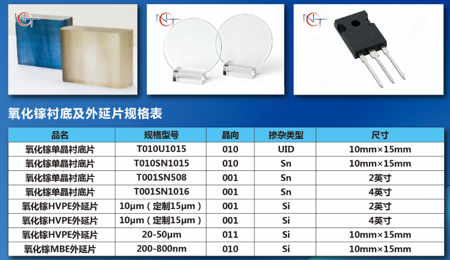
Gallium Oxide single crystal substrate and epitaxial wafer:Provide NCT’s high-quality Gallium Oxide single crystal substrates, epitaxial and device products, and can provide a variety of customized product models, which are applied in research and development work in different fields such as device verification, epitaxial growth, and chip processing.
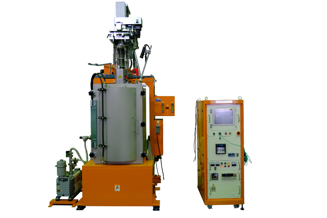
Gallium Oxide crystal growth furnace(EFG/VB):Imported crystal growth equipment from Japan can achieve the growth of ultra wide bandgap Gallium Oxide single crystal semiconductor materials using EFG and VB method. The equipment can meet the growth requirements of 2-6 inch single crystal materials and also meet the customized design needs of users.
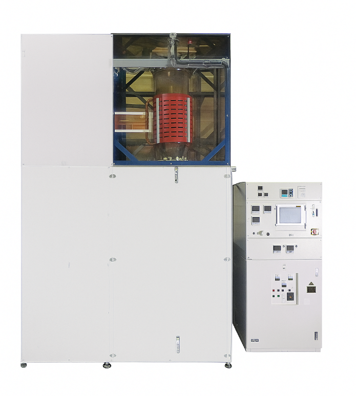
Silicon Carbide crystal growth furnace(PVT/TSSG):Imported crystal growth equipment from Japan can achieve the growth of Silicon Carbide single crystal semiconductor materials using PVT and TSSG method. The equipment can meet the growth requirements of 6-8 inch single crystal materials and also meet the customized design needs of users.
BOOTH:96
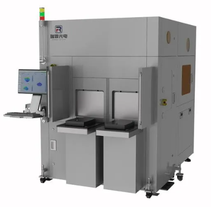
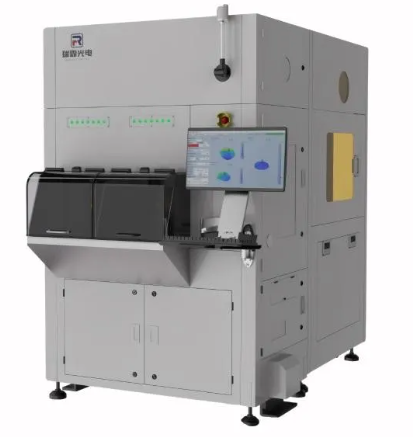
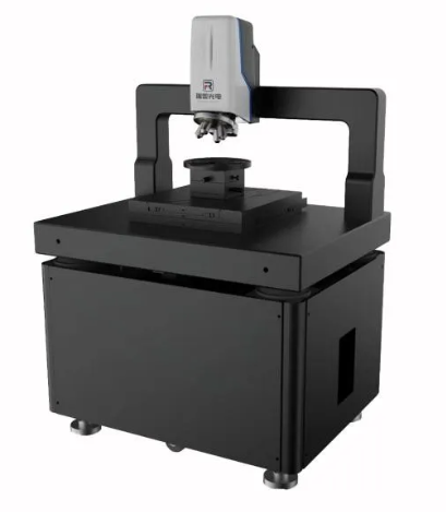
Suzhou Raphael Optech Co., Ltd. is a high-tech enterprise specializing in the research, development, and manufacturing of advanced optical inspection and imaging systems. The company was registered in August 2018 in Taicang, Suzhou, with an R&D center and branch office in Shanghai, and a liaison office in Shenzhen.
Raphael boasts a research team led by PhDs from prestigious universities including Tsinghua University, Soochow University, and University of Shanghai for Science and Technology. To date, the company has been granted more than 50 invention and utility model patents, along with 10 software copyrights.
Facing the industrial wave of fourth-generation semiconductors represented by Gallium Oxide (Ga₂O₃), Raphael has proactively deployed core inspection technologies, focusing on key challenges such as microscopic morphology, stress distribution, and defect identification, driving the intelligent upgrade of the wide-bandgap semiconductor industry.
As an ultra-wide bandgap semiconductor, Ga₂O₃ offers high breakdown field strength (4.8 eV), excellent thermal stability, and low-cost fabrication, showing tremendous potential in high-power electronics, solar-blind UV detectors, and energy-efficient power grids. However, microscopic defects generated during production can significantly reduce device performance and yield. Traditional inspection methods suffer from low efficiency, sample damage, and difficulty in real-time monitoring.

BOOTH:98
Hebei Poshing Electronic Technology Co., Ltd. is a state-owned high-tech enterprise specialized in the research and development and production of semiconductor epitaxy materials. It belongs to China Electronics Technology Group Co., LTD., formerly known as the epitaxy Research Group of the 13th Research Institute of China Electronics Technology Group Co., LTD. It began to research and development of epitaxy materials in 1962 and established Poshing Company in 2000. It has more than 20 years of research and development and large-scale production experience in the epitaxy industry. Up to now, Poshing Company has formed an annual output of 8.4 million epitaxial sheet production capacity, epitaxial material output, market share in the domestic industry are leading, has become the domestic epitaxial material production enterprises leading.
Silicon Carbide (SiC) Epitaxial Wafers:The 6-inch and 8-inch SiC homoepitaxial wafers are third-generation wide bandgap semiconductor materials, featuring a wide bandgap, high carrier velocity, and excellent thermal conductivity. They hold significant strategic importance, and their production technology is currently a key focus of scientific and technological competition worldwide.At present, applications of SiC wide bandgap semiconductor materials require the growth of epitaxial layers on substrates before they can be used. SiC homoepitaxial wafers are ideal materials for manufacturing high-power and high-voltage devices. Compared with traditional silicon power devices, SiC power devices offer superior performance and higher power density. They are widely used in LEDs, solar and wind power generation, new energy vehicles, aerospace, rail transportation, high-voltage power transmission and distribution, and various detectors.
Alliance Event
The Alliance is attending this conference with the goal of further enhancing industry visibility and strengthening the professional influence of Gallium Oxide materials, while leveraging the conference platform to gain more comprehensive insights into the semiconductor industry, continuously improving the depth and foresight of its services. Through exchanges and mutual learning across the industry chain, the Alliance will continue to enhance its capabilities and promote the development of a more professional Gallium Oxide industry service platform.
During the conference, the Asian Gallium Oxide Alliance will also host a “Follow for Gifts” lottery activity at Booth 91! Participants simply need to follow the Alliance’s official WeChat public account and video channel to enter the lottery for a chance to win attractive prizes such as data cables, mouse pads, fridge magnets, and more.
We warmly invite everyone to visit the booth to participate in the lottery and engage in on-site exchanges, making your conference experience richer and more rewarding.
It is worth noting that the Alliance has also specially organized a member-focused interview session, inviting representatives from key areas in the Gallium Oxide field, including materials, equipment, epitaxy, and devices. The purpose is to present cutting-edge discussions and provide deeper industry insights.
The interview content will be compiled and released after the conference—stay tuned!
Highlights from Previous Editions