Paper Sharing
【Domestic Papers】Self-powered solar-blind UV photodetector based on Cs₂CdCl₄/β-Ga₂O₃ heterojunction
日期:2025-12-02阅读:546
Researchers from the Zhengzhou University have published a dissertation titled "Self-powered solar-blind UV photodetector based on Cs2CdCl4/β-Ga2O3 heterojunction in Chinese Science Bulletin.
Background
Solar-blind ultraviolet (200–280 nm) detection has broad application prospects in fire warning, UV alarms, and optical communications. Traditional photomultiplier tubes are bulky and power-consuming; wide-bandgap semiconductors are costly; and alloy materials often suffer from phase separation. β-Ga₂O₃ is an ideal material, but it typically requires an external bias and lacks self-powered capability. Three-dimensional perovskites exhibit poor stability, while the all-inorganic two-dimensional perovskite Cs₂CdCl₄ offers solar-blind absorption. However, due to its low solubility, it is difficult to fabricate high-quality thin films via solution processing.
Abstract
Solar-blind ultraviolet (UV) light (200–280 nm) is strongly absorbed by the ozone layer and cannot reach the Earth’s surface. Consequently, solar-blind UV photodetectors possess unique advantages of low false-alarm rates and strong anti-interference capabilities, demonstrating broad application prospects in fire early warning, UV warning systems, and wireless optical communication. Although photomultiplier tubes offer high signal-to-noise ratios and high gain, they suffer from inherent drawbacks such as high cost, high power consumption, and bulky size. With the advancement of semiconductor technology, despite solar-blind UV detectors based on wide-band gap semiconductor materials having made rapid progress, the current wide-bandgap semiconductor materials still face the limitations of complex fabrication processes and susceptibility to phase separation. β-Ga2O3, featuring a direct bandgap of 4.9 eV, high carrier mobility, and low-cost fabrication, emerges as an ideal candidate material for solar-blind UV photodetectors. Nevertheless, β-Ga2O3-based detectors with metal-semiconductor-metal structures require external bias for operation, inevitably increasing device power consumption. Due to the persistent challenges in achieving shallow acceptor doping in β-Ga2O3, there are currently no reports of self-powered, homogeneous p-n junction solar-blind UV photodetectors. As an alternative approach, integrating it with other wide-bandgap materials to form β-Ga2O3 heterojunction self-powered photodetectors presents a viable solution.
Despite metal halide perovskites possessing tunable band gaps, high absorption coefficients, and long carrier diffusion lengths, the poor stability due to organic ammonium salts, inability to extend the optical bandgap into the solar-blind UV region, and prevalent halide ion migration constrain their practical applications. Low-dimensional perovskite derivatives can spatially isolate ion migration channels, largely mitigating the detrimental effects of ion migration. The two-dimensional (2D) Ruddlesden-Popper phase all-inorganic cadmium-based halide Cs2CdCl4 possesses unique solar-blind UV absorption characteristics, making it a promising candidate for integration with β-Ga2O3 to construct self-powered photodetectors responsive exclusively to solar-blind UV light. However, the extremely low solubility of CsCl and CdCl2 in organic solvents makes it difficult to prepare high-quality Cs2CdCl4 films via conventional solution methods. In contrast, the vapor co-deposition method offers significant advantages such as solvent-free processing, precise control of evaporation rates, and high reproducibility, making it particularly suitable for such poorly soluble materials.
This study systematically investigated the crystal structure, electronic band characteristics, and crystal growth behavior of the all-inorganic 2D Ruddlesden-Popper perovskite Cs2CdCl4. For the first time, uniform, dense, high-crystallinity Cs2CdCl4 thin films were fabricated using vapor co-deposition technology. Combined density functional theory calculations and experimental characterization confirmed its ultra-wide bandgap, enabling selective absorption of solar-blind UV radiation. By integrating Cs2CdCl4 films with β-Ga2O3, a type-II band-aligned heterojunction photodetector was successfully constructed. Under 0 V bias and 265 nm solar-blind UV illumination, the device achieved a linear dynamic range of 70.37 dB, responsivity of 11.96 mA W−1, and specific detectivity of 3.7 × 10¹¹ Jones. Furthermore, utilizing the device as a photosensing pixel in a UV imaging system successfully reconstructed a high-fidelity “UV” pattern under 265 nm illumination, while exhibiting no response to 360 nm non-solar-blind UV light, fully validating its selective detection capability for solar-blind UV light. This work provides an important reference for the material design and device development of next-generation solar-blind UV detectors.
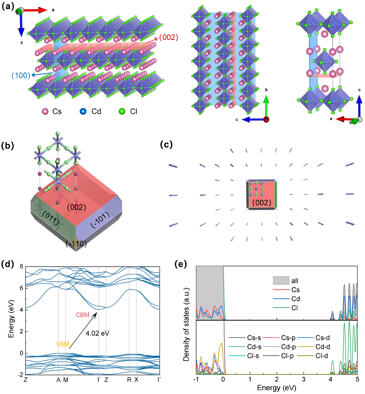
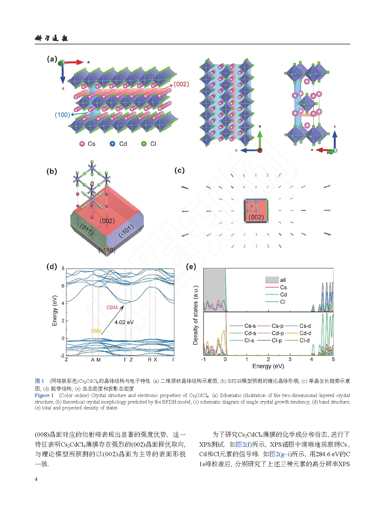
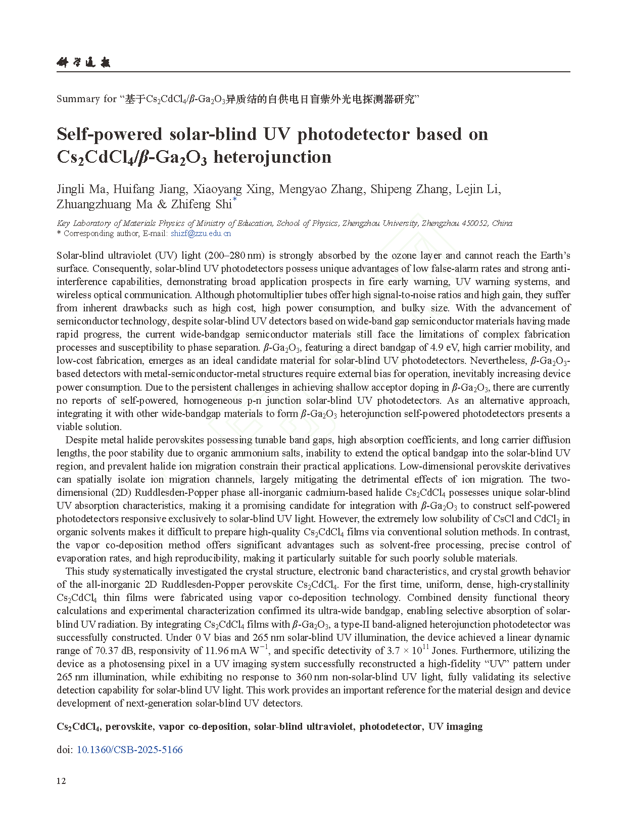
Figure 1. Crystal structure and electronic properties of Cs2CdCl4. (a) Schematic illustration of the two-dimensional layered crystal structure; (b) theoretical crystal morphology predicted by the BFDH model; (c) schematic diagram of single crystal growth tendency; (d) band structure; (e) total and projected density of states
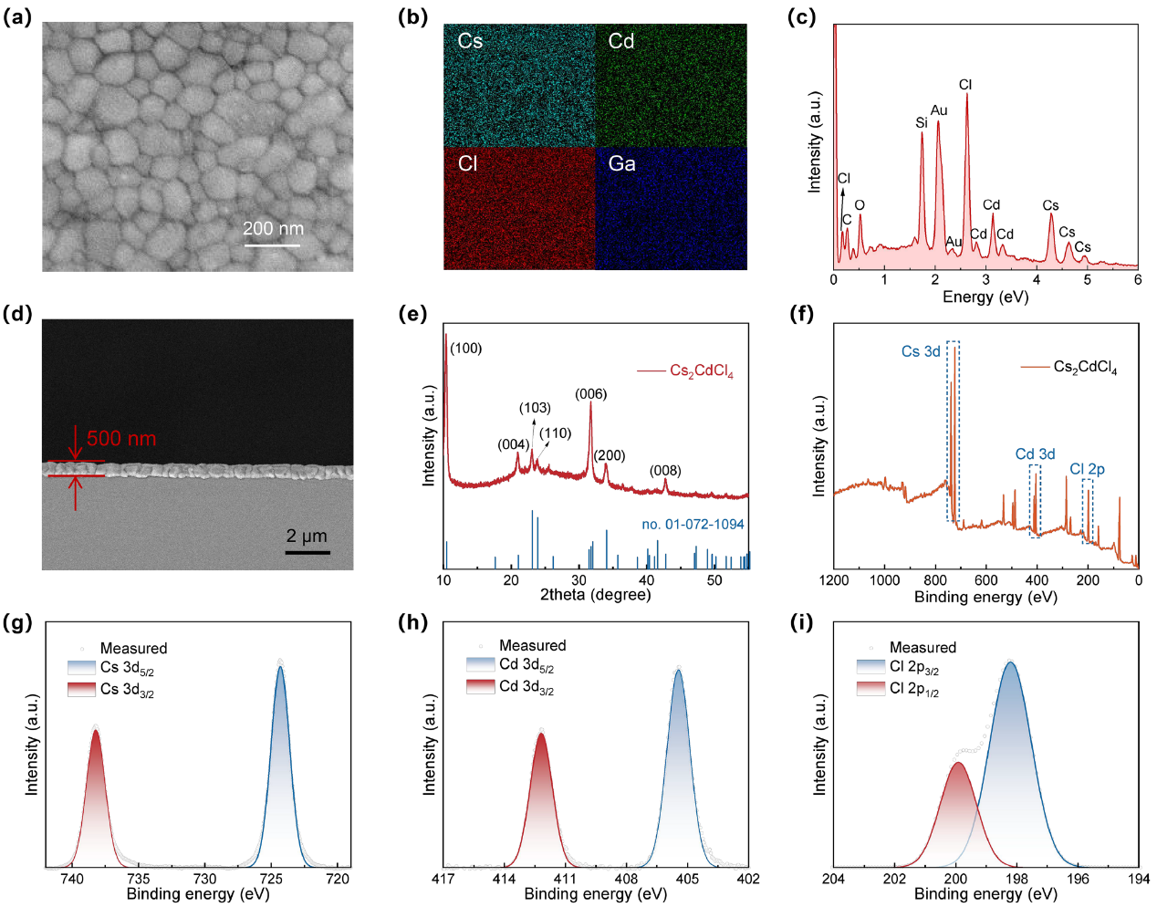
Figure 2. Morphological, structural, and compositional characterization of the Cs2CdCl4 thin films. (a) Top-view SEM image; (b) elemental mapping; (c) EDS spectrum; (d) cross-sectional SEM image; (e) XRD pattern compared with the standard reference for tetragonal Cs2CdCl4; (f) XPS survey spectrum; high resolution XPS spectra of (g) Cs 3d, (h) Cd 3d, and (i) Cl 2p
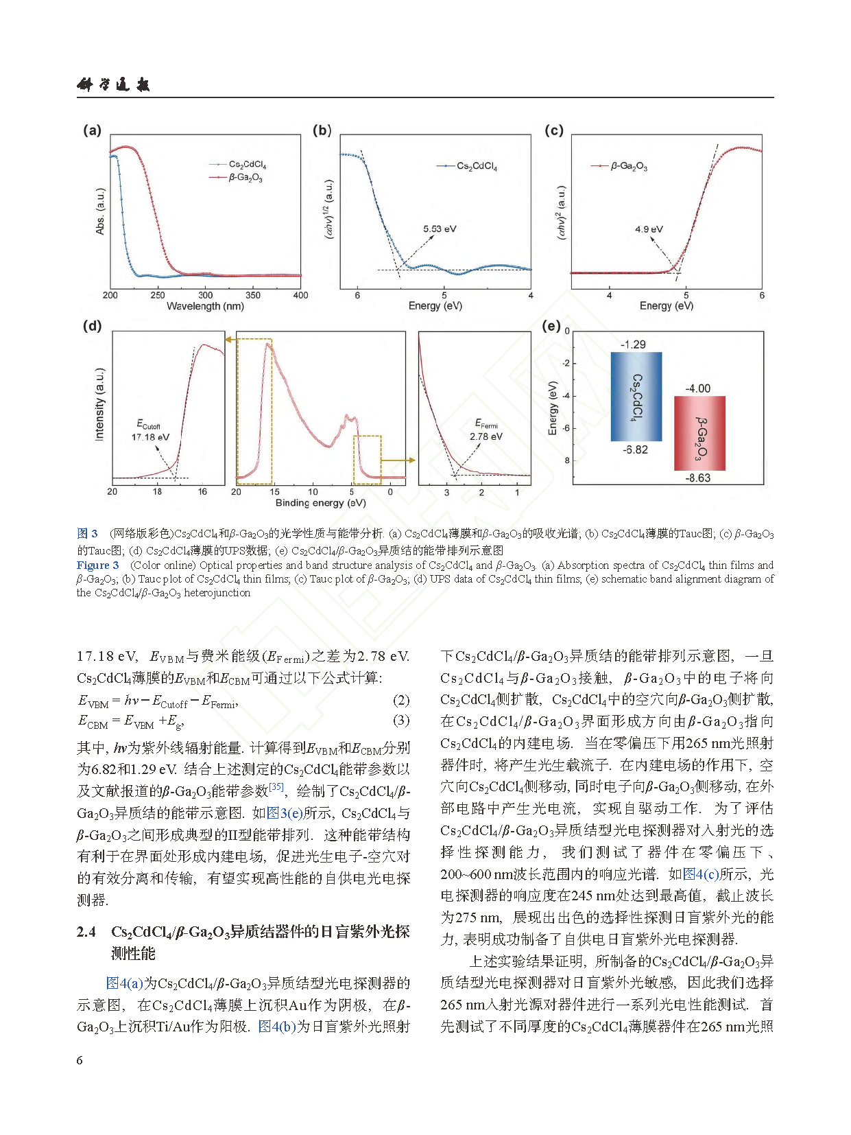
Figure 3. Optical properties and band structure analysis of Cs2CdCl4 and β-Ga2O3. (a) Absorption spectra of Cs2CdCl4 thin films and β-Ga2O3; (b) Tauc plot of Cs2CdCl4 thin films; (c) Tauc plot of β-Ga2O3; (d) UPS data of Cs2CdCl4 thin films; (e) schematic band alignment diagram of the Cs2CdCl4/β-Ga2O3 heterojunction
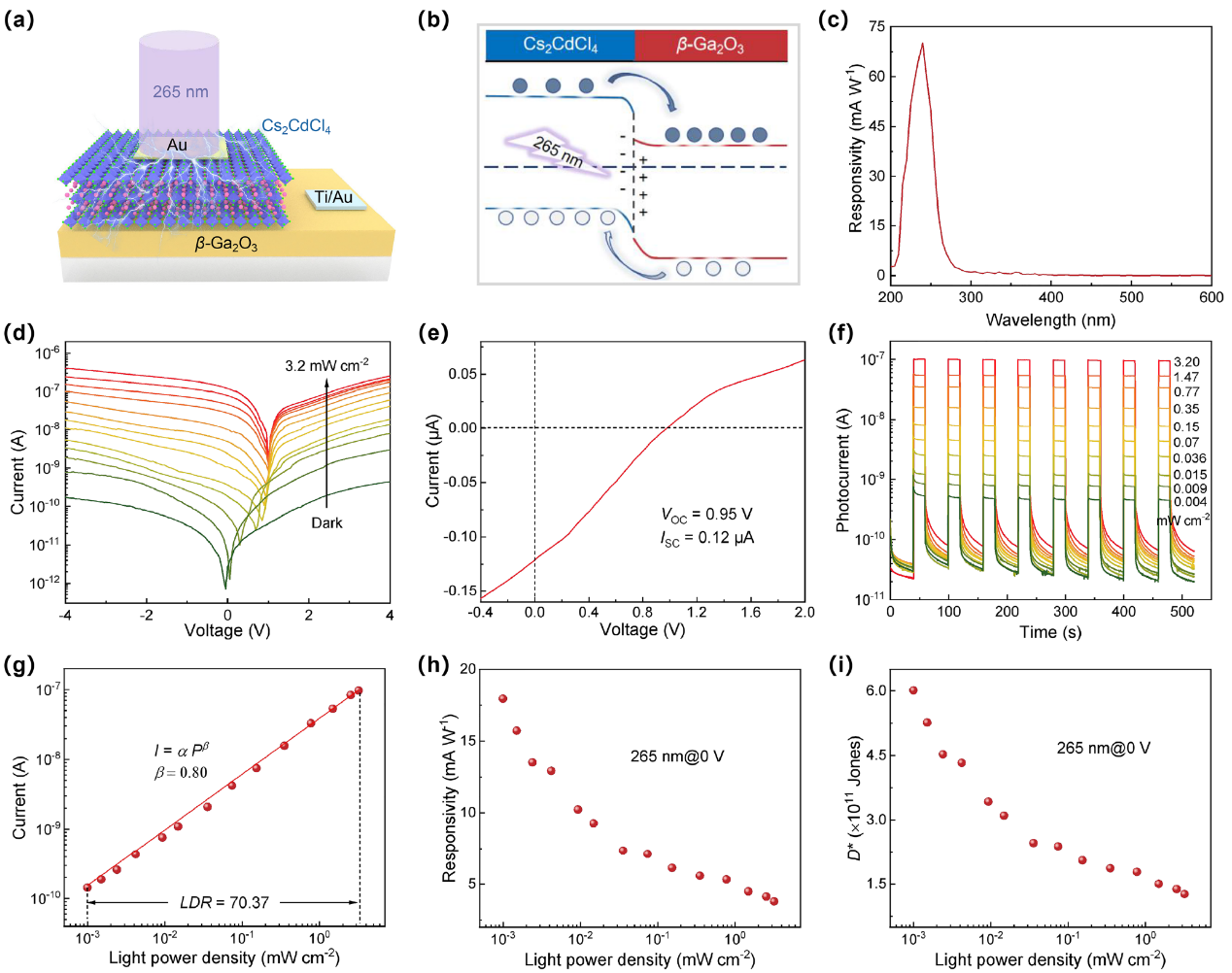
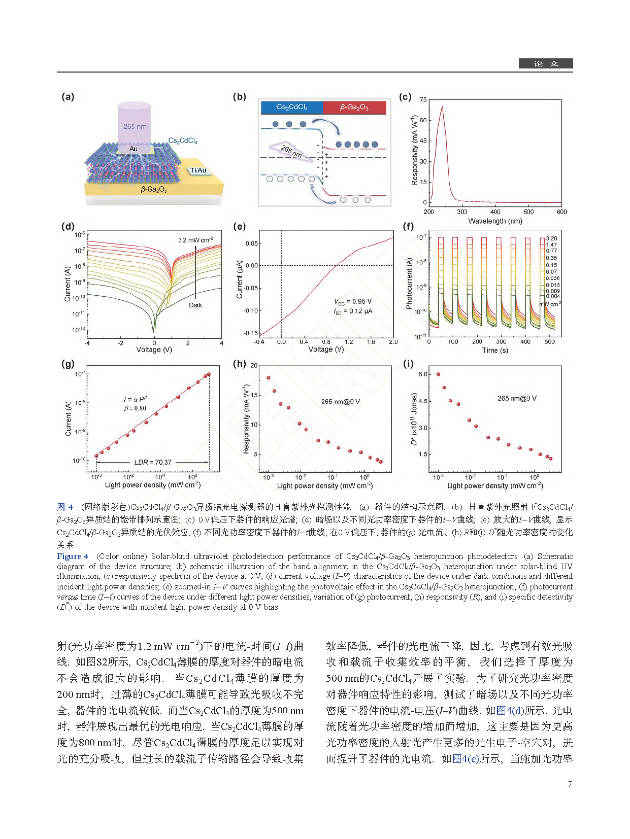
Figure 4. Solar-blind ultraviolet photodetection performance of Cs2CdCl4/β-Ga2O3 heterojunction photodetectors. (a) Schematic diagram of the device structure; (b) schematic illustration of the band alignment in the Cs2CdCl4/β-Ga2O3 heterojunction under solar-blind UV illumination; (c) responsivity spectrum of the device at 0 V; (d) current-voltage (I–V) characteristics of the device under dark conditions and different incident light power densities; (e) zoomed-in I−V curves highlighting the photovoltaic effect in the Cs2CdCl4/β-Ga2O3 heterojunction; (f) photocurrent versus time (I−t) curves of the device under different light power densities; variation of (g) photocurrent, (h) responsivity (R), and (i) specific detectivity (D*) of the device with incident light power density at 0 V bias
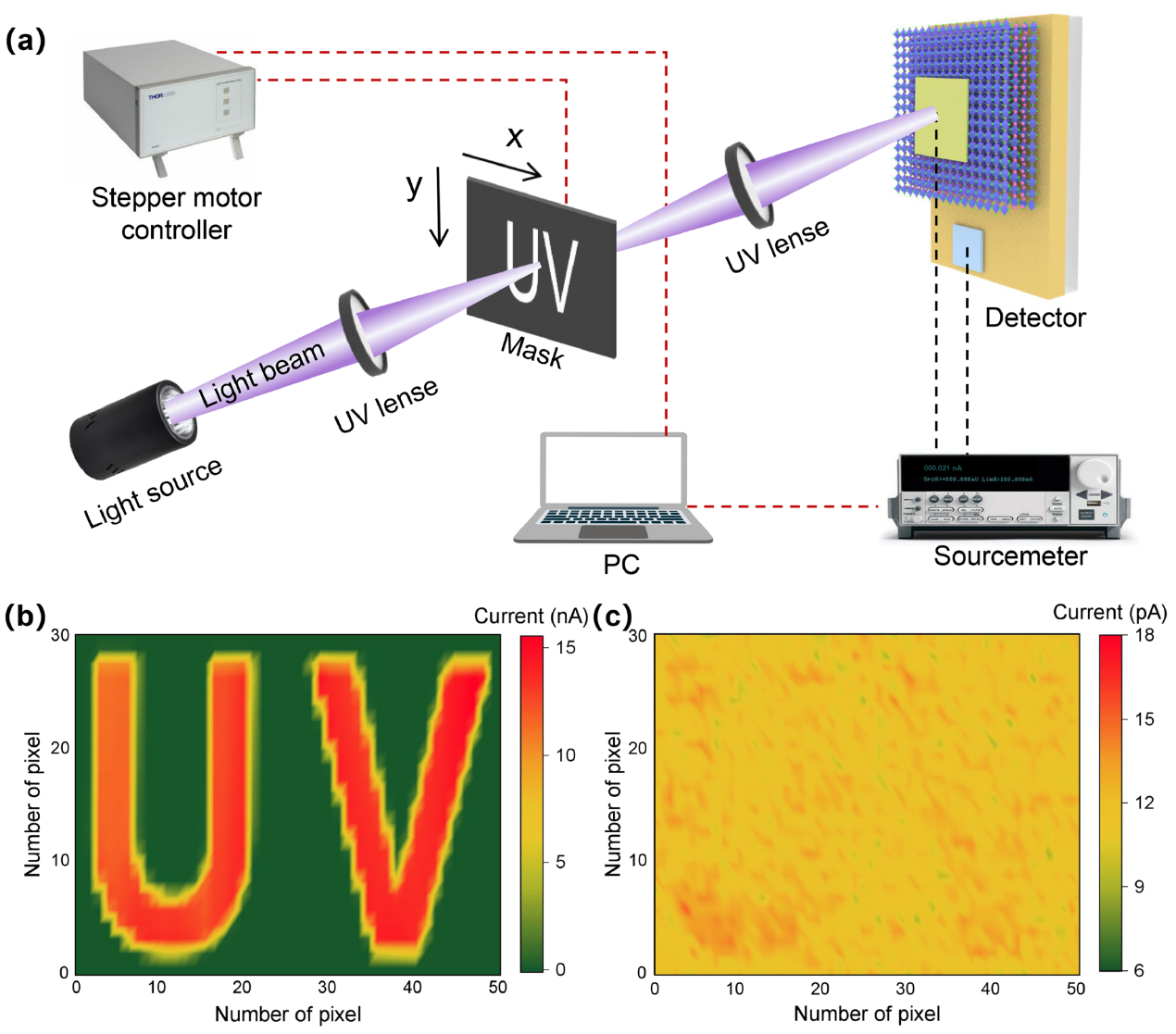
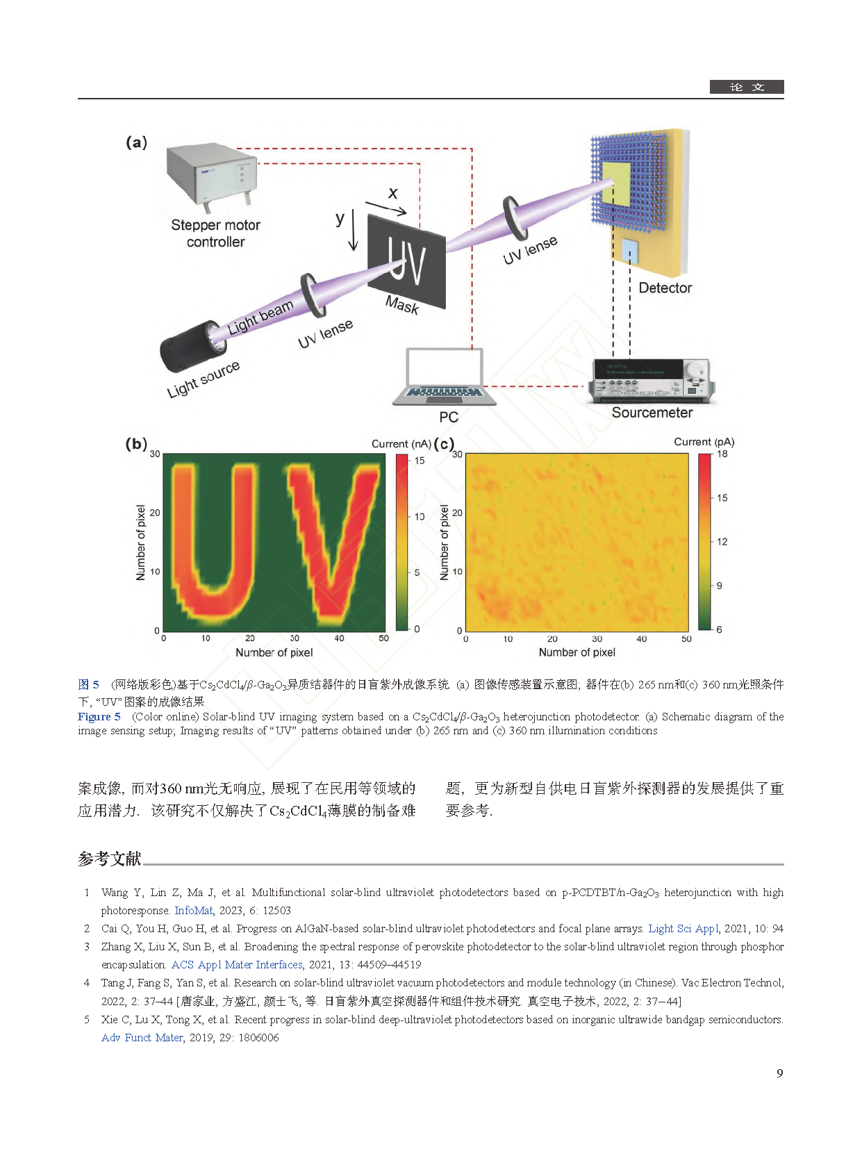
Figure 5. Solar-blind UV imaging system based on a Cs2CdCl4/β-Ga2O3 heterojunction photodetector. (a) Schematic diagram of the image sensing setup; Imaging results of “UV” patterns obtained under (b) 265 nm and (c) 360 nm illumination conditions
DOI:
doi.org/10.1360/CSB-2025-5166