Paper Sharing
【Member Papers】2.3 kV low leakage vertical (001) β-Ga₂O₃ diodes enabled by a synergistic guard ring and beveled field plate
日期:2025-12-02阅读:601
Researchers from the Xidian University and Xi’an Jiaotong University have published a dissertation titled "2.3 kV low leakage vertical (001) β-Ga2O3 diodes enabled by a synergistic guard ring and beveled field plate " in Journal of Vacuum Science & Technology A
Project Support
This work was supported by the Joint Funds of the National Natural Science Foundation of China U23A20367.
Background
β-Ga₂O₃ is an ultrawide-bandgap (4.5–4.9 eV) semiconductor with a high theoretical breakdown field (~8 MV/cm) and excellent potential for low-cost, high-quality homoepitaxy using melt-grown single-crystal substrates. These properties make it a promising candidate for next-generation high-voltage and high-temperature power devices. However, a major challenge limiting β-Ga₂O₃ vertical devices from reaching their material-limited performance (Baliga’s figure of merit) is poor electric-field control at device edges, compounded by the difficulty of p-type doping, which prevents conventional edge-termination techniques like FLRs and JTEs. Alternative strategies—such as field plates (FP), beveled field plates (BFP), mesa terminations, ion-implanted guard rings (GR), and capping layers—have been explored to reduce edge-field crowding and improve breakdown voltage and leakage characteristics. The combination of BFPs with ion-implanted GRs shows promise in managing edge electric fields effectively, enabling high-performance β-Ga₂O₃ power devices.
Abstract
This study presents a vertical (001) β-Ga2O3 Schottky barrier diode (SBD) incorporating a composite edge termination structure, which combines a nitrogen-implanted guard ring (GR) with a small-angle beveled field plate (BFP). Leveraging technology computer-aided design simulations grounded in semiconductor physics, we developed and optimized the device's geometric structure. Integration of GR with BFPs enables suppression of the anode-edge electric-field peak without degrading the favorable forward conduction characteristics. Thanks to this optimized termination design, the fabricated diode achieves a breakdown voltage (Vbr) of 2.3 kV—6.5 times higher than that of nonterminated devices—along with a specific on-resistance (Ron,sp) of 3.19 mΩ cm2. These properties yield a high Baliga's figure of merit of 1.71 GW/cm2. Furthermore, at a reverse bias of −1500 V, the device demonstrates a low leakage current density of less than 1 μA/cm2. This work presents a feasible approach to improve the performance of β-Ga2O3 SBDs, paving the way for their adoption in power electronics.
Conclusion
In summary, the incorporation of a nitrogen-implanted guard ring (GR) and a shallow-bevel field plate (BFP) effectively mitigates anode-edge electric field crowding in the β-Ga2O3 Schottky barrier diode. The β-Ga2O3 GR/BFP-SBD exhibits a low Ron,sp of 3.19 mΩ cm2 and a high Vbr of 2338 V, yielding a high BFOM of 1.71 GW/cm2 and maintaining a low leakage current density of 1 μA/cm2 at a reverse voltage of −1500 V. This composite termination structure achieves a 6.5-fold increase in breakdown voltage with virtually no compromise in forward characteristics. This work provides an effective composite terminal technology for electric field regulation of vertical β-Ga2O3 SBD and demonstrates the promising prospects of high-performance multi-kV β-Ga2O3 devices.
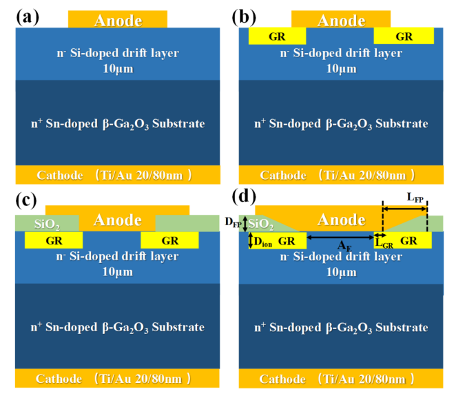
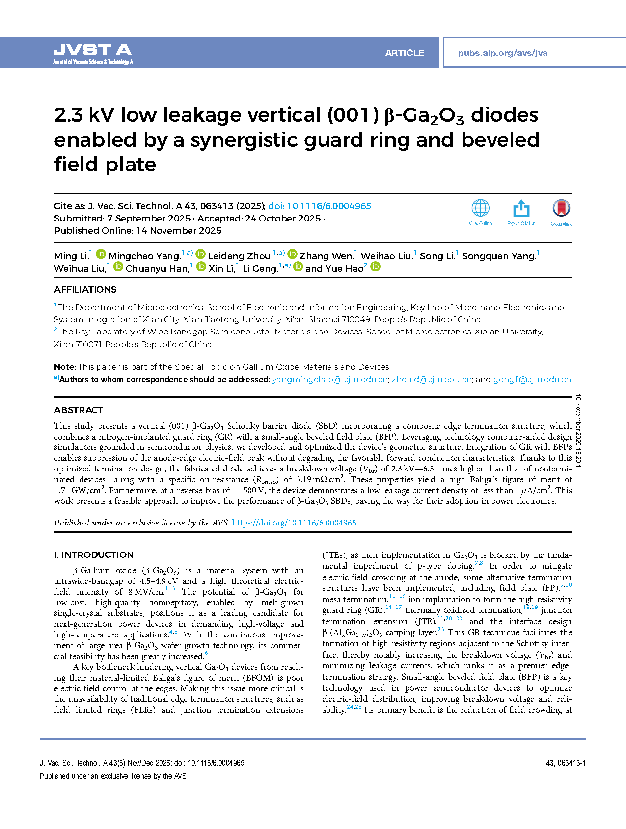
FIG. 1. Schematic cross sections of β-Ga2O3. (a) Ref-SBDs, (b) GR-SBDs, (c) GR/FP-SBDs, and (d) GR/BFP-SBDs.
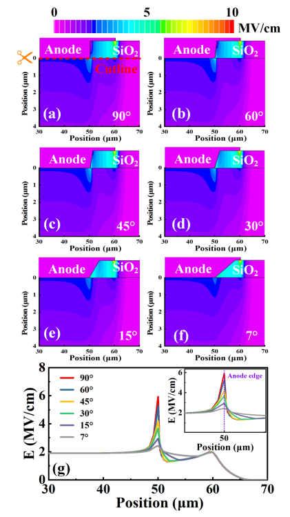
FIG. 2. (a)–(f) Dependence of the simulated 2D electric field distribution on different bevel angles of FPs under a reverse bias of 1000 V. (g) Extracted horizontal electric field profiles at the β-Ga2O3 surface for FPs with different bevel angles.
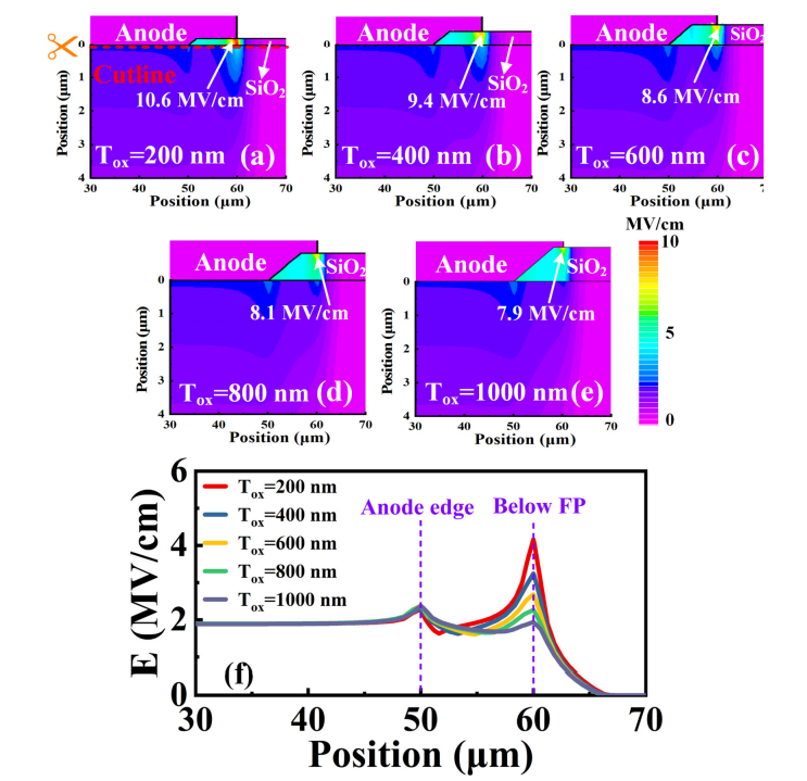
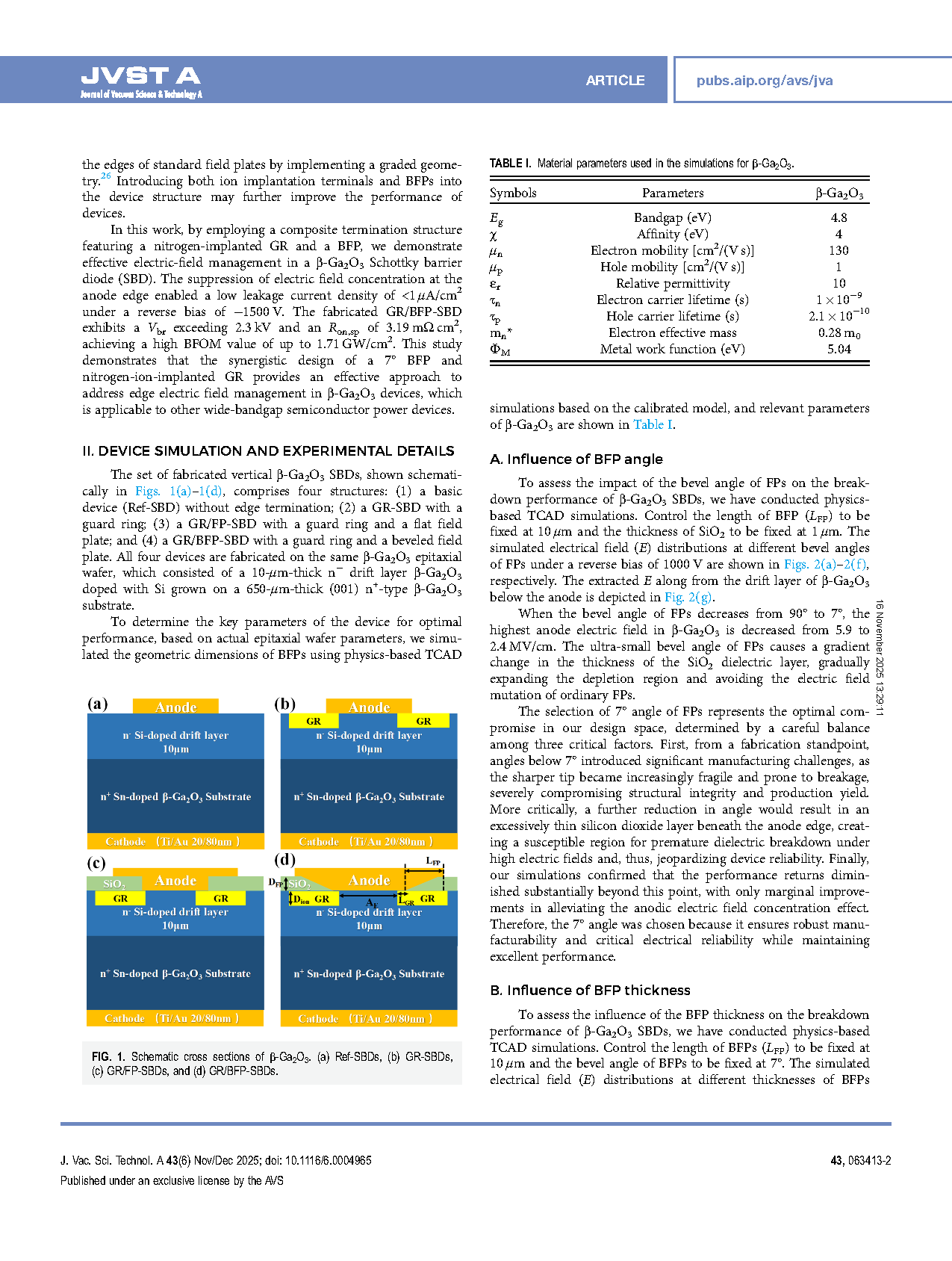
FIG. 3. (a)–(e) Dependence of the simulated 2D electric field distribution on different thicknesses of BFPs under a reverse bias of 1000 V. (f) Extracted horizontal electric field profiles at the β-Ga2O3 surface for different thicknesses of BFPs.
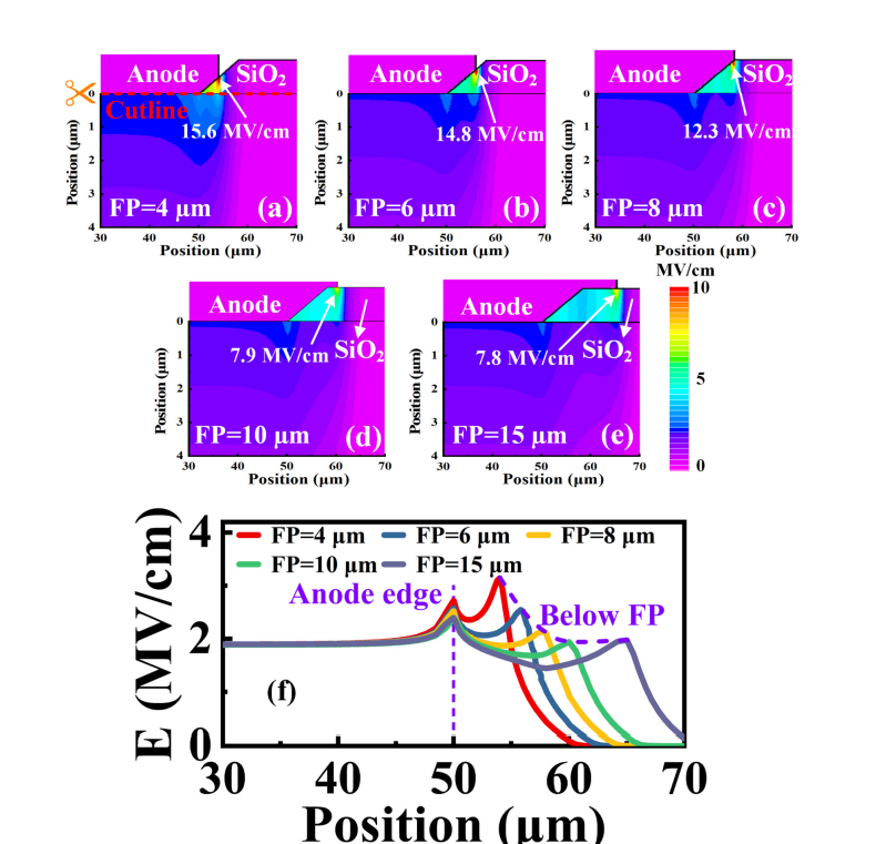
FIG. 4. (a)–(e) Dependence of the simulated 2D electric field distribution on different lengths of BFPs under a reverse bias of 1000 V. (f) Extracted horizontal electric field profiles at the β-Ga2O3 surface for different lengths of BFPs.
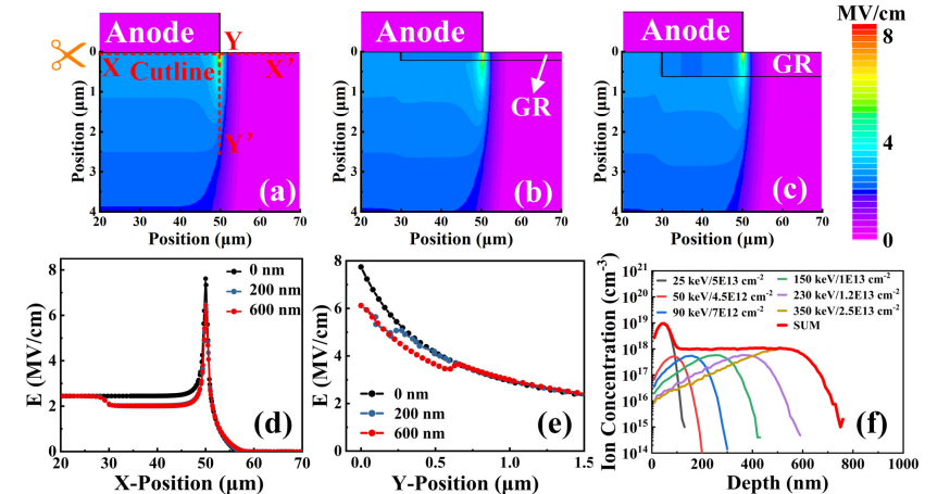
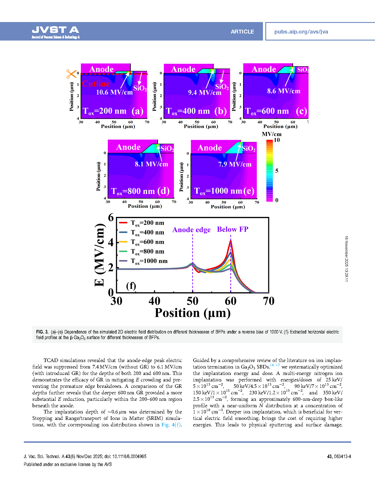
FIG. 5. (a)–(c) Dependence of the simulated 2D electric field distribution on different thicknesses of GR under a reverse bias of 1000 V. Extracted electric field profiles at the β-Ga2O3 surface (d) under anode and (e) below anode corner edge for different thicknesses of GR. (f) SRIM simulations of ion profiles in β-Ga2O3 by multi-energy nitrogen ion implantation.
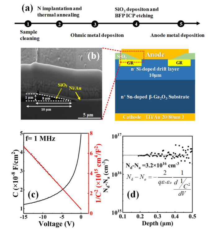
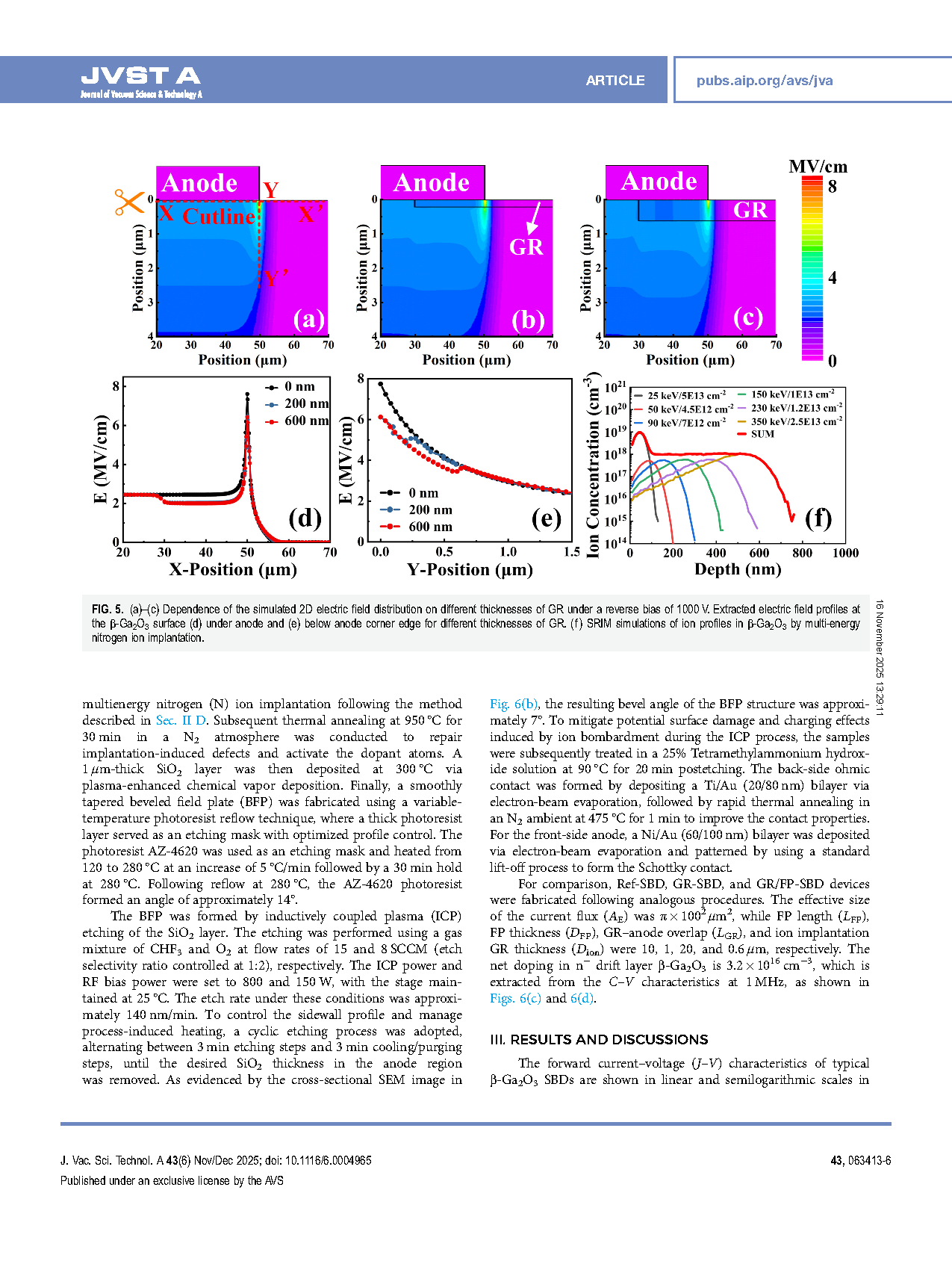
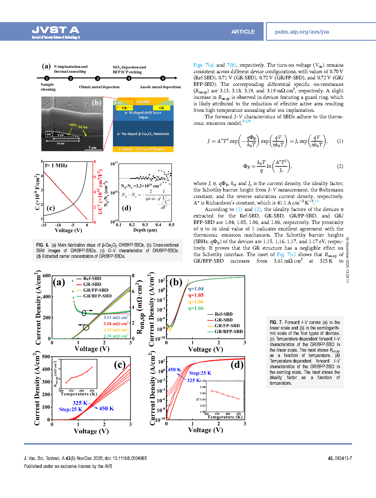
FIG. 6. (a) Main fabrication steps of β-Ga2O3 GR/BFP-SBDs. (b) Cross-sectional SEM images of GR/BFP-SBDs. (c) C–V characteristics of GR/BFP-SBDs. (d) Extracted carrier concentration of GR/BFP-SBDs.
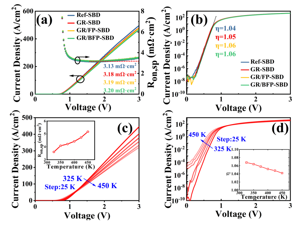
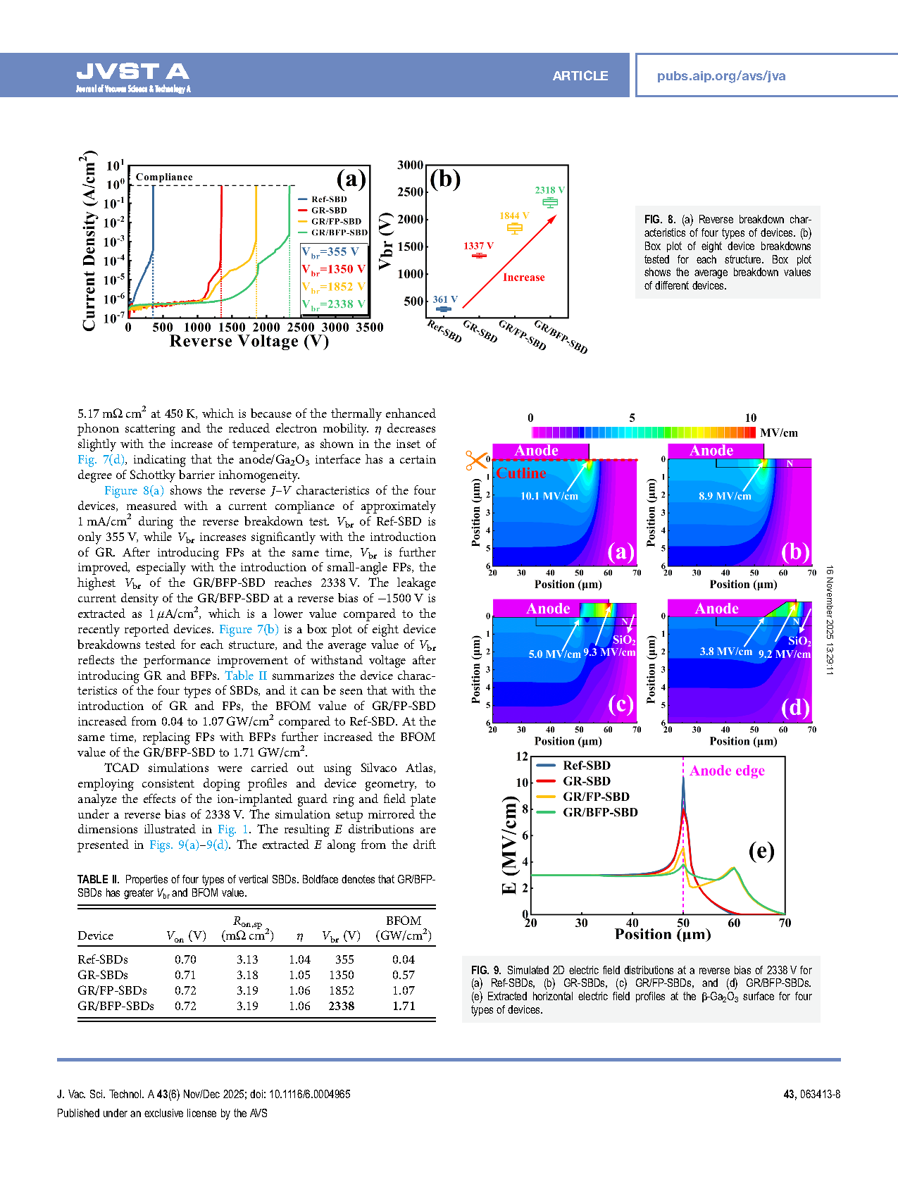
FIG. 7. Forward I–V curves (a) in the linear scale and (b) in the semilogarithmic scale of the four types of devices. (c) Temperature-dependent forward I–V characteristics of the GR/BFP-SBD in the linear scale. The inset shows Ron,sp as a function of temperature. (d) Temperature-dependent forward I–V characteristics of the GR/BFP-SBD in the semilog scale. The inset shows the ideality factor as a function of temperature.
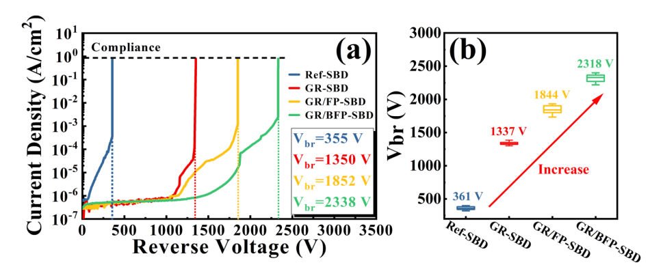
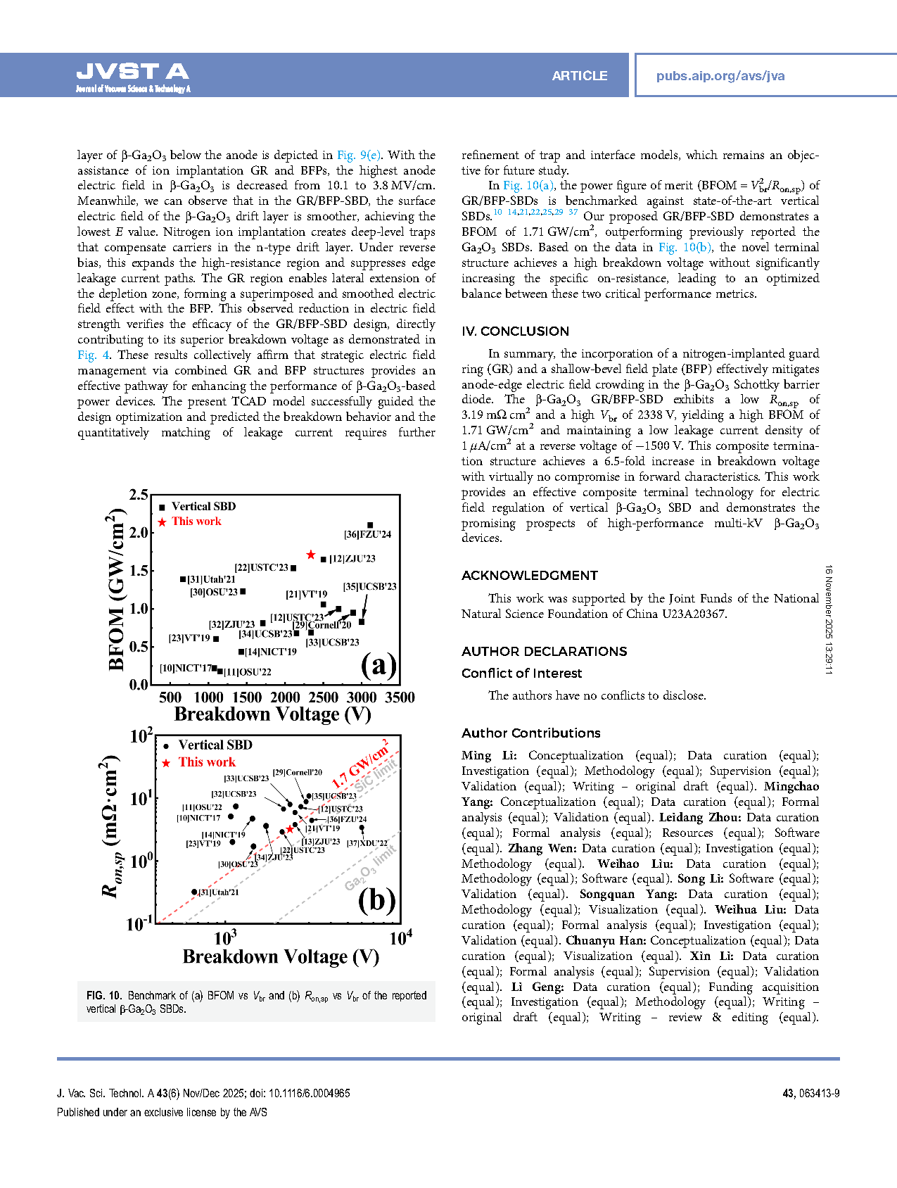
FIG. 8. (a) Reverse breakdown characteristics of four types of devices. (b) Box plot of eight device breakdowns tested for each structure. Box plot shows the average breakdown values of different devices.
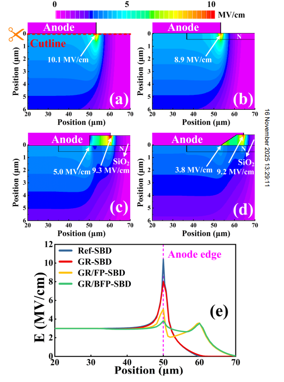
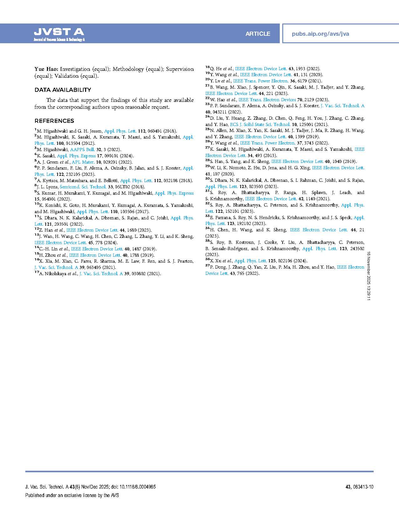
FIG. 9. Simulated 2D electric field distributions at a reverse bias of 2338 V for (a) Ref-SBDs, (b) GR-SBDs, (c) GR/FP-SBDs, and (d) GR/BFP-SBDs. (e) Extracted horizontal electric field profiles at the β-Ga2O3 surface for four types of devices.
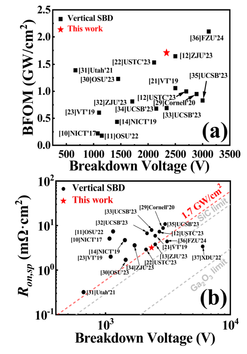
FIG. 10. Benchmark of (a) BFOM vs Vbr and (b) Ron,sp vs Vbr of the reported vertical β-Ga2O3 SBDs.
DOI:
doi.org/10.1116/6.0004965