Paper Sharing
【Member Papers】Improving interfacial thermal conductivity by constructing covalent bond between Ga₂O₃ and SiC
日期:2025-12-02阅读:619
Researchers from the Fudan University have published a dissertation titled "Improving interfacial thermal conductivity by constructing covalent bond between Ga2O3 and SiC" in Nature Communications.
Acknowledgements
W.D. acknowledges support from the National Key R&D Program of China (2022YFA1203100) and the National Natural Science Foundation of China (62574209); H.P.M. acknowledges support from the Science and Technology Innovation Plan of Shanghai Science and Technology Commission (No. 21DZ1100800, 23ZR1405300); Q.J.Z. acknowledges support from the Science and Technology Innovation Plan of Shanghai Science and Technology Commission (20501110700, and 20501110702); Q.L.Y. acknowledges support from the National Natural Science Foundation of China (52302202); N.J. acknowledges support from the Yongjiang Talent Introduction Program of Ningbo (2021A-037-C and 2021A-108-G).
Background
Since modern electronic devices have evolved toward the higher power, frequency and temperature capabilities, wide-bandgap semiconductor materials have garnered significant research interest due to their exceptional physical properties. Silicon carbide (SiC) is widely utilized in high-power applications because of its wide bandgap of 3.2 eV and low conduction loss. However, the low saturated electron mobility still limits the effectiveness of SiC in high-frequency domains. In contrast, gallium nitride (GaN) offers notable advantages under high-frequency conditions but lacks the ability to produce self-supporting substrates, which restricts its use in high-power scenarios. Gallium oxide (Ga₂O₃), a semiconductor with an ultra-wide bandgap (approximately 4.8 eV), has attracted considerable attention for its potential in high-voltage power and high-frequency electronic devices. Ga₂O₃ exhibits exceptionally high critical breakdown field (projected to be up to 8 MV/cm) and low on-resistance, which can significantly reduce losses in power devices. Furthermore, it has a high saturation electron velocity (∼2 × 107 cm/s) and an impressive Johnson’s figure of merit (JFOM), thus being an ideal candidate for high-frequency applications.
Abstract
Gallium oxide (Ga₂O₃) is emerging as a promising semiconductor for next-generation power and radio-frequency electronics due to its ultra-wide bandgap and high breakdown field. Yet, its intrinsic thermal conductivity is extremely low, which causes severe self-heating and limits reliable device operation. A common approach to overcome this challenge is to integrate Ga₂O₃ with substrates of high thermal conductivity such as silicon carbide (SiC). However, weak bonding across the heterojunction interface creates large thermal resistance, preventing efficient heat removal. Here we show that constructing strong covalent bonds between Ga₂O₃ and SiC through an engineered interlayer enables both structural compatibility and efficient phonon transport. This bonding strategy increases the interface thermal conductivity to 162 MW/m²·K, the highest value reported for Ga₂O₃ heterostructures. Infrared thermography confirms that the bonded devices exhibit a temperature reduction of up to 29 °C under high power densities, demonstrating significant mitigation of self-heating. These findings establish a practical route for enhancing thermal management in Ga₂O₃ electronics and highlight the importance of interfacial bonding design. Beyond Ga₂O₃, this approach may be extended to other wide-bandgap semiconductors where thermal bottlenecks constrain device performance.
Conclusion
In summary, the heat dissipation of a Ga₂O₃ film on the SiC substrate was successfully enhanced through a simple route consisting of the formation of covalent bonds, which is compatible with existing production lines. Furthermore, we conducted TCAD simulations by treating the ITC derived from the experimental tests on both covalent and VdW contacts as a variable. The results showed that the increase of ITC from 17.5 to 162.1 MW/m²·K significantly reduced the impact of the self-heating effect, leading to an 83 mA/mm improvement in the maximum output current of the MOSFET along with a notable drop in the local junction temperature. By optimizing the heat treatment process, the microstructure at the interface was adjusted so as to facilitate the formation of robust covalent bonds and the creation of effective phonon transport channels. Time-domain thermoreflectance (TDTR) measurements revealed that the ITC between Ga₂O₃ and SiC after the covalent bond formation achieved a remarkable value of 162 MW/m²·K, representing a nine-fold increase compared to the van der Waals (VdW) force connection (17.5 MW/m²·K). Furthermore, the NJTM approach was applied to enhance the ITC whereby the bonding temperature of samples exposed to intense illumination was reduced by approximately 29 °C relative to those with VdW connections. This significantly enhanced performance and reliability of the appliance. Moreover, in-situ XPS studies during the deep etching confirmed the formation of SiO₂ upon heat treatment. The Si-O and Si-C covalent bonds at the interface ensured the effective phonon transport, in which the SiO₂ layer acted as a phonon bridge between Ga₂O₃ and SiC. MD simulations further confirmed that the formation of covalent bonds considerably increased the heat flow at the interface, thereby reducing its thermal resistance. The ITC value between Ga₂O₃ and SiO₂ was enhanced by approximately 40 times compared to that in the case of VdW forces, reaching an impressive value of 919.9 MW/m²·K. Through the comprehensive experimental and theoretical analyses, it was concluded that introducing a SiO₂ layer between Ga₂O₃ and SiC was conducive to the formation of covalent bonding, significantly enhancing heat diffusion and providing a promising strategy to address the low thermal conductivity of Ga₂O₃.
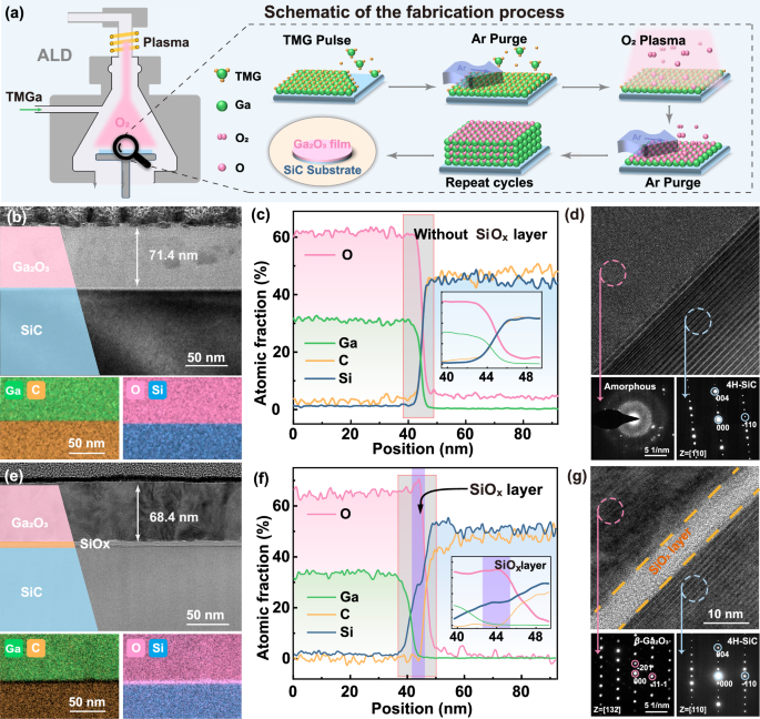
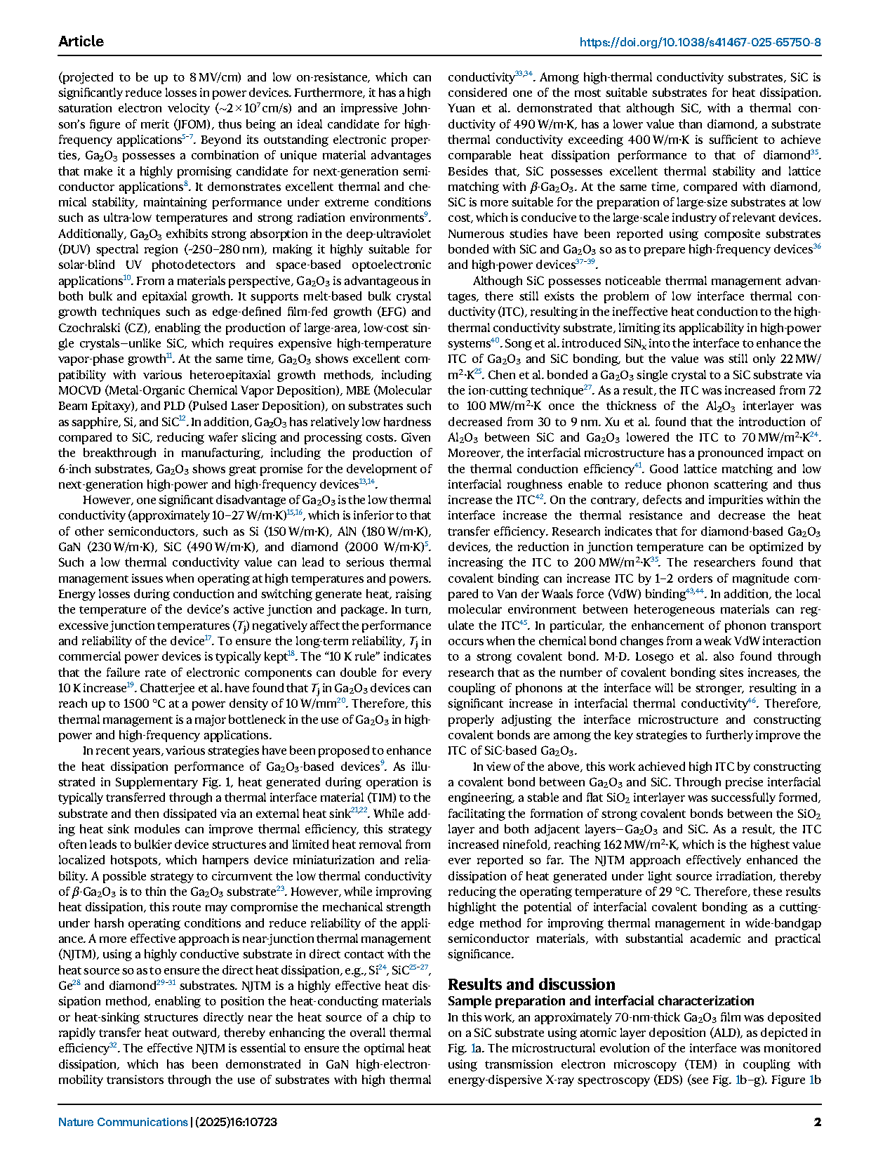
Fig. 1: TEM images of Ga₂O₃/SiC and Ga₂O₃/SiO₂/SiC heterojunctions before and after annealing. a Schematic of the fabrication process. b Cross-sectional TEM image and corresponding EDS maps of the untreated sample. c EDS line scans of the cross-section. d HRTEM micrograph of Ga₂O₃/SiC heterojunction interface and SAED pattern (e) Cross-sectional TEM image and corresponding EDS maps of the sample annealed for 120 min at 1173 K. f EDS line scans of the cross-section. g HRTEM micrograph of Ga₂O₃/SiO2/SiC heterojunction interface and SAED pattern.
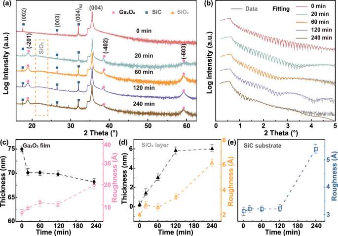
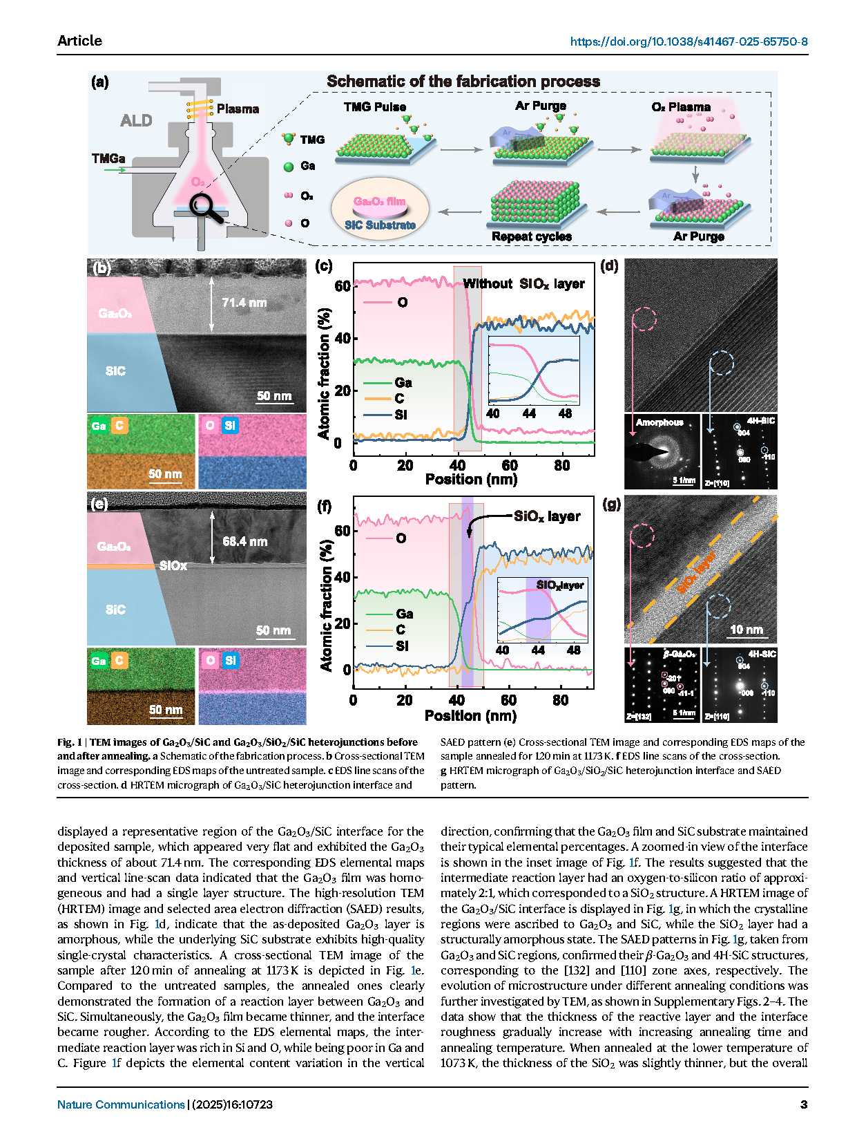
Fig. 2: Structural characterization of as-deposited and annealed samples by XRD and XRR analyses. (a) XRD patterns and (b) Measured and fitted XRR curves of the as-deposited and annealed samples. (c–e) The extracted XRR data for the corresponding layers and the error bars represent standard deviation.

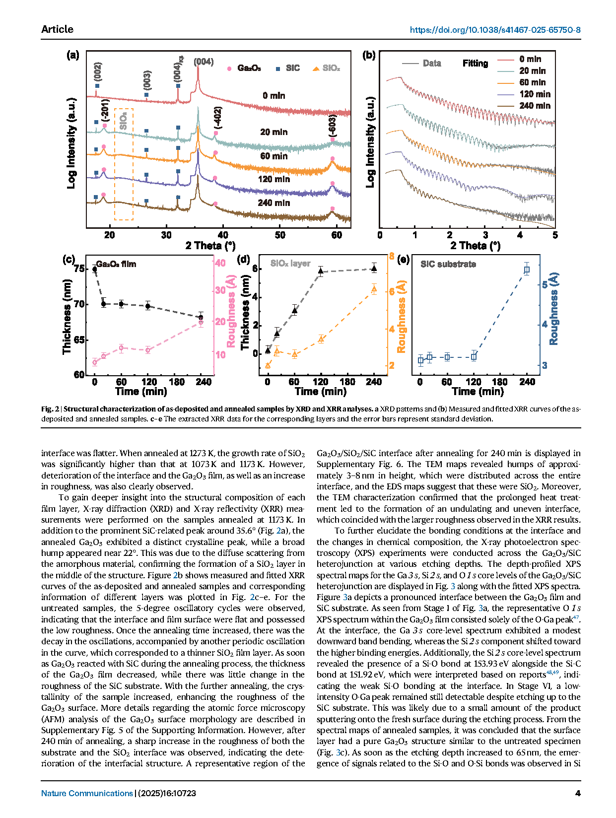
Fig. 3: Depth-resolved XPS analysis and structural evolution of Ga₂O₃/SiC heterojunctions before and after annealing. a Depth-profiled XPS spectral maps corresponding to Si 2 s and O 1 s core-level features across the Ga₂O₃/SiC heterojunction in the untreated sample. b The corresponding Si 2 s and O 1 s XPS peaks at different etching depths. c Depth-profiled XPS spectral maps corresponding to Si 2 s and O 1 s core-level features across the Ga₂O₃/SiC heterojunction in the sample annealed for 120 min. d The corresponding Si 2 s and O 1 s XPS peaks at different etching depths. e Schematic crystal structures of β-Ga₂O₃ and amorphous Ga₂O₃ after high-temperature thermalization. f Radial distribution function of amorphous Ga₂O₃. g Heterogeneous interface of Ga₂O₃ and 4H-SiC before and after the reaction. h Si-O bond ratios vary with reaction time.
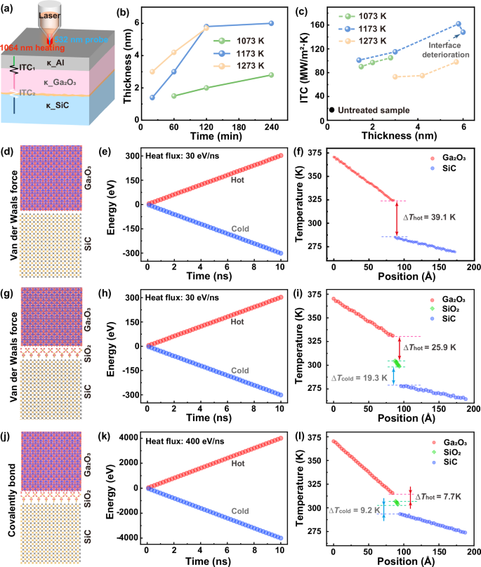
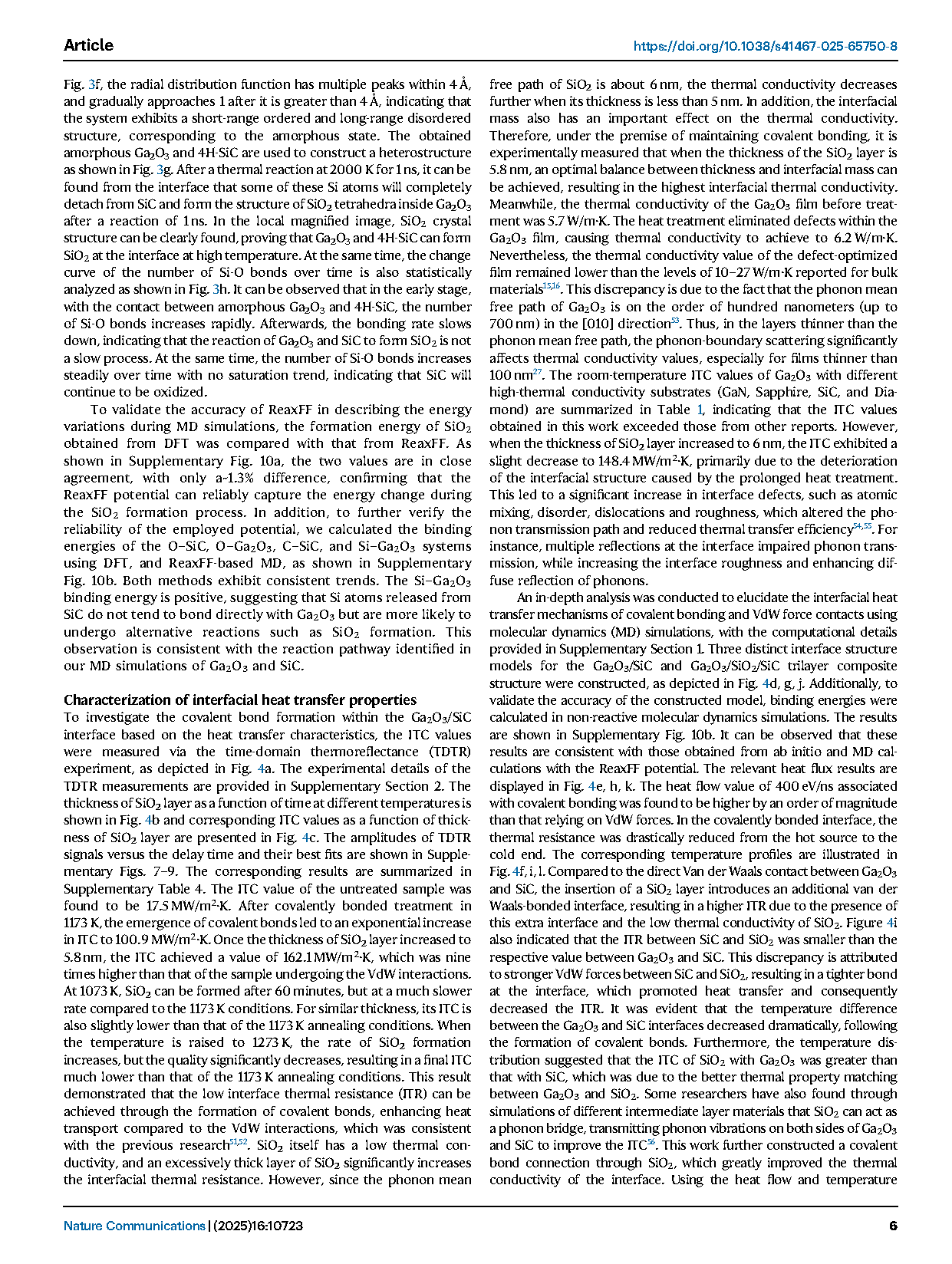
Fig. 4: The TDTR experimental and MD simulation analysis of interfacial thermal transport across Ga₂O₃/SiC and Ga₂O₃/SiO₂/SiC heterojunctions with different bonding configurations. a Schematic diagram of the sample structure and the TDTR experiment. b The thickness of SiO2 layer as a function of time at different temperatures. c The ITC values established via the TDTR measurements at different thickness of SiO2 layer. d, g, j Structural modeling for molecular dynamics calculations at the Ga₂O₃/SiC interface bonded by (d) VdW and Ga₂O₃/SiO2/SiC interface bonded by (g) VdW and (j) covalent interactions. The accumulative energy of the heat source and heat sink of the Ga₂O₃/SiC interface bonded by (e) VdW and Ga₂O₃/SiO2/SiC interface bonded by (h) VdW and (k) covalent interactions. Typical temperature profiles of the Ga₂O₃/SiC interface bonded by (f) VdW and Ga₂O₃/SiO2/SiC interface bonded by (i) VdW and (l) covalent interactions.
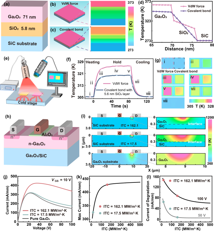
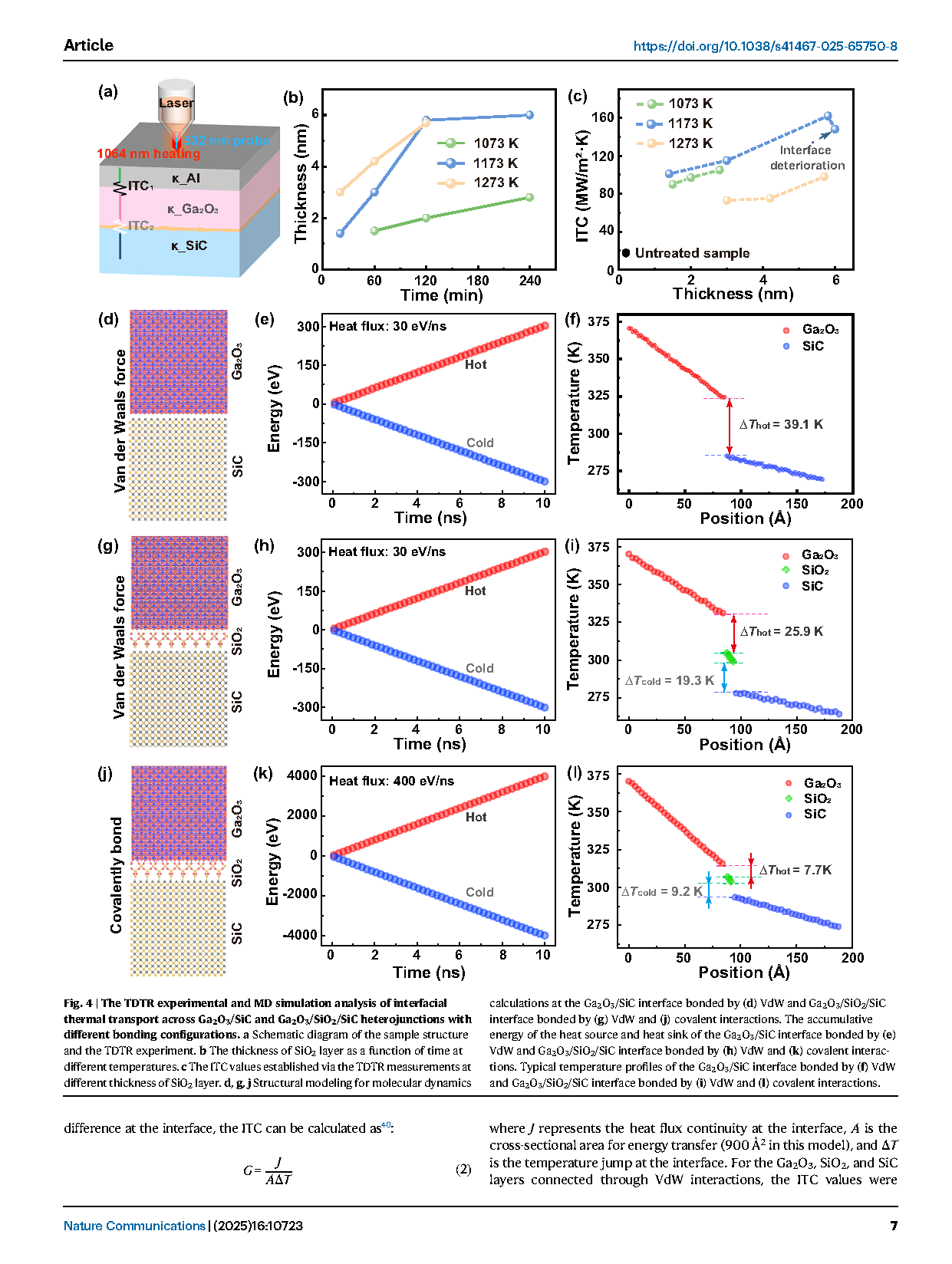
Fig. 5: Multiscale simulation and experimental characterization of interfacial thermal transport across Ga₂O₃/SiC heterojunctions. a Schematic diagram of Finite Element Method simulations. b, c The comparison of heat dissipation capability based on simulated profiles. d The temperature profiles of the different interface. e Schematic diagram of the infrared thermography measurements. f The surface temperature evolution of VdW force and covalent bond samples as a function of time, captured with an infrared camera. g Corresponding temperature distributions of the samples surface captured in situ at different time. h Schematic illustrations of the MOSFET device. i Simulated 2D heat maps of the cross-section of the MOSFET device. j ID as a function of VD at different ITC values. k Maximum ID as a function of ITC values. l ID of degradation as a function of ITC values.
DOI:
doi.org/10.1038/s41467-025-65750-8