Paper Sharing
【Member Papers】High-performance β-Ga₂O₃ vertical diodes integrating metal-interlayer-semiconductor architecture and mesa termination
日期:2025-12-14阅读:575
Researchers from the Xidian University have published a dissertation titled "High-performance β-Ga2O3 vertical diodes integrating metal-interlayer-semiconductor architecture and mesa termination" in Applied Physics Letters.
Background
β-Ga₂O₃, with its ultra-wide bandgap of 4.8–4.9 eV, exceptionally high critical electric field, and large Baliga figure of merit, has become a leading candidate for next-generation high-voltage power devices. The availability of low-defect, melt-grown native substrates further enables significant progress in device scalability and performance. However, the lack of stable p-type doping limits the realization of conventional p–n junctions, making metal–semiconductor and heterojunction structures the primary device options. These structures face inherent limitations such as high reverse leakage or elevated turn-on voltages. To overcome these constraints, introducing an ultrathin interfacial layer to form a metal–interlayer–semiconductor (MIS) configuration has emerged as an effective strategy for suppressing leakage, increasing barrier height, and improving interface quality. Meanwhile, device terminal engineering—including field plates, guard rings, and mesa termination—plays a critical role in electric-field modulation, among which mesa termination has been shown to significantly enhance breakdown performance through optimized edge-field distribution.
Although various interlayer materials, such as Al₂O₃, TiOₓ, and BN, have been investigated, the systematic utilization of intrinsic p-type NiO as an ultrathin insertion layer in vertical Ga₂O₃ MIS diodes remains limited. Its potential to enhance barrier height, reduce interface trap density, and improve overall electric-field management when combined with mesa termination has not been fully explored. Developing a MIS structure that incorporates a high-quality ultrathin NiO interlayer together with a self-aligned mesa terminal structure is therefore of strong interest for achieving high breakdown voltage, low leakage current, and stable conduction characteristics. This work aims to address this need by demonstrating a high-performance vertical Ga₂O₃ MIS diode architecture that integrates thermally oxidized ultrathin NiO with mesa termination, enabling significant improvements in rectification performance and breakdown capability for advanced power electronics applications.
Abstract
In this Letter, we report on high-performance β-Ga2O3 metal-interlayer-semiconductor (MIS) diodes featuring anode self-aligned mesa terminations and ultra-thin NiO as interlayers. The polycrystalline NiO interlayer was formed by thermal oxidation of a 5-nm Ni film deposited by e-beam evaporation and the mesa termination was fabricated by inductively coupled plasma etching. High-resolution transmission electron microscopy revealed a polycrystalline structure of the NiO and a perpendicular sidewall angle of approximately 84.6° at the mesa region. The 40-μm-radius mesa metal-interlayer-semiconductor Schottky barrier diodes achieves a low turn-on voltage of 1 V and a high breakdown voltage of 2.45 kV, while maintaining a decent specific on-resistance of 4.2 mΩ·cm2, yielding a power figure of merit of 1.43 GW/cm2, which is one of the highest among those reported state-of-the-art Ga2O3 MIS and mesa-termination diodes. Additionally, high on/off ratio of 1011, negligible C–V and I–V hysteresis curves, ideality factor of 1.2, and subthreshold swing of 74 mV/dec are demonstrated, all attributable to the well-defined NiO/Ga2O3 interface and the high crystal quality. The fabricated β-Ga2O3 MIS diodes with mesa termination show good switching performance, further promoting Ga2O3 technology for next-generation power electronics.
Conclusion
In conclusion, by integrating ultra-thin thermally oxidized NiO as an interlayer and anode self-aligned mesa termination, we have fabricated high-performance vertical β-Ga₂O₃ MMIS SBDs with a high breakdown voltage (BV) of 2.45 kV and a low specific on-resistance (Ron,sp) of 4.2 mΩ·cm², surpassing the previously reported power figures of merit (P-FOMs) of MIS and MMS diodes. Owing to the enhanced barrier height of 1.15 eV provided by the interlayer and the high-quality interface, the diodes show an ultra-high rectification ratio of 10¹¹, a low subthreshold swing (SS) of 74 mV/dec, as well as negligible hysteresis in bidirectional I–V and C–V measurements. The lower leakage current compared to MMS diodes and the excellent high-temperature stability highlight the advantages of the MIS structure and demonstrate the strong potential of the MMIS structure for next-generation power rectifiers.
Project Support
This research is supported by the National Natural Science Foundation of China (NSFC) under Grant Nos. 62222407 and 62421005, and by the Guangdong Basic and Applied Basic Research Foundation under Grant No. 2023B1515040024. Additional support was provided by the Deanship of Scientific Research (DSR) at King Abdulaziz University, Jeddah, Saudi Arabia, which partially funded this project under Grant No. IPP: 1424-135-2025, along with technical assistance.
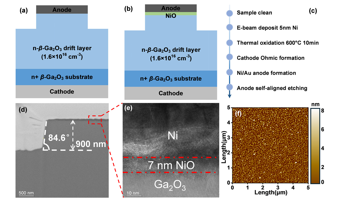
FIG. 1. Cross-sectional schematics of (a) the MMS and (b) the MMIS diodes. (c) The fabrication process of the MMIS diode. HR-TEM images of (d) cross section and (e) mag nified interface of MMIS SBD reveal a perpendicular mesa termination and a polycrystalline structure of NiO interlayer. (f) AFM image of the NiO surface morphology prepared by thermal oxidation.

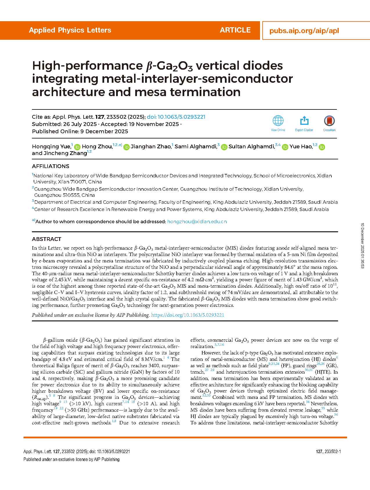
FIG. 2. (a) C–V and 1/C2–V curves of MMIS diode at 100kHz with extracted Vbi of 1.7 V and net doping concentration of 1.6×1016 cm 3. (b) Bidirectional C–V sweep illustrates negligible hysteresis.
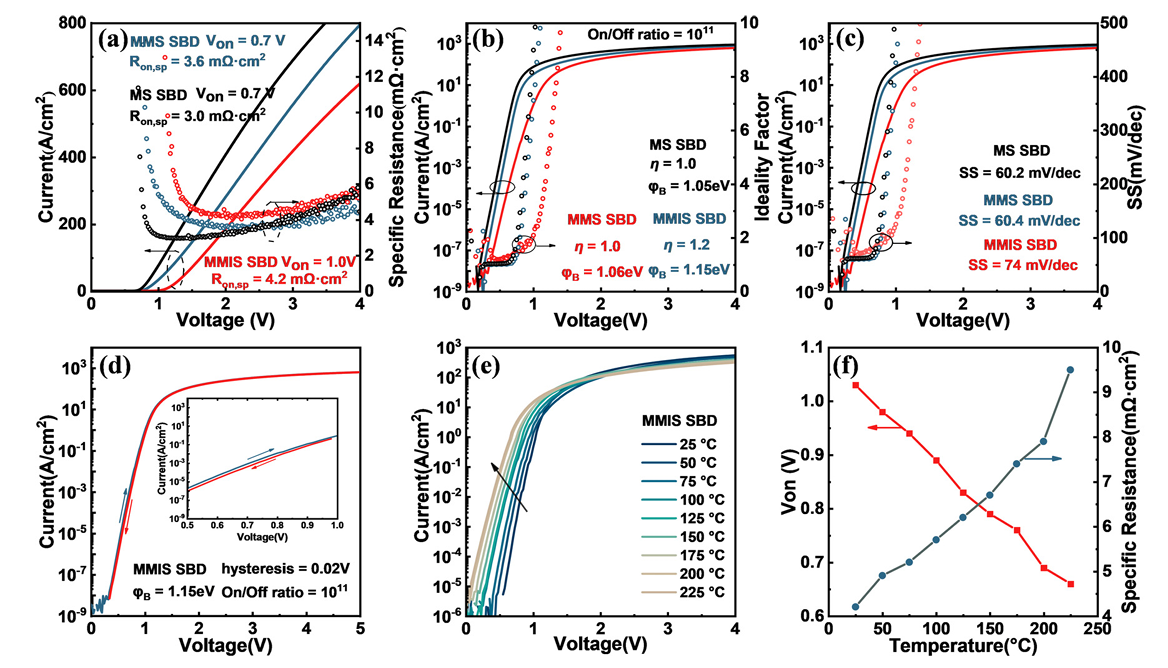
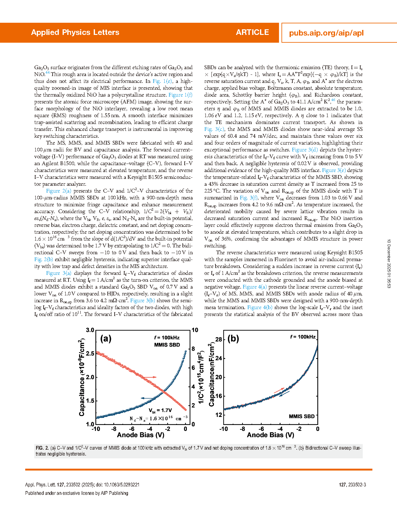
FIG. 3. (a) Forward I–V characteristics and differential Ron,sp, (b) log-scale I–V curves and ideality factor with extracted φB and on/off ratio, (c) log-scale I–V curves and SS of MS, MMS, and MMIS SBDs. (d) Bidirectional I–V sweeps of MMIS diode with low hysteresis of 0.02V. (e) Temperature-related forward I–V characteristics of MMIS diode at elevated T from 25 to 225 °C with steps of 25 °C. (f) Summary of Von and Ron,sp variation with temperature.
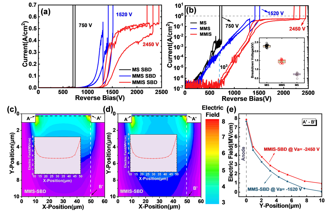
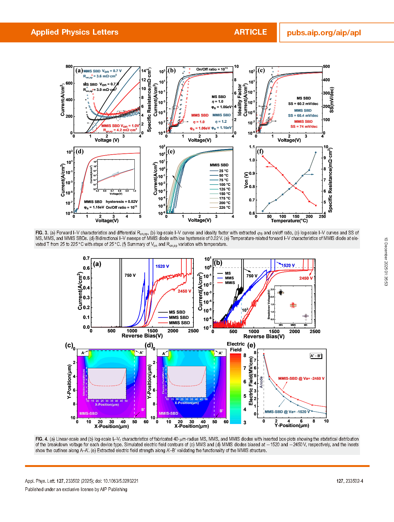
FIG. 4. (a) Linear-scale and (b) log-scale Ir–Vr characteristics of fabricated 40-μm-radius MS, MMS, and MMIS diodes with inserted box-plots showing the statistical distribution of the breakdown voltage for each device type. Simulated electric field contours of (c) MMS and (d) MMIS diodes biased at 1520 and 2450V, respectively, and the insets show the cutlines along A–A’. (e) Extracted electric field strength along A’–B’ validating the functionality of the MMIS structure.
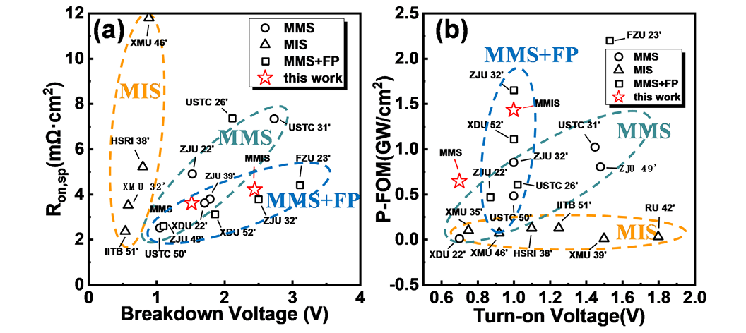
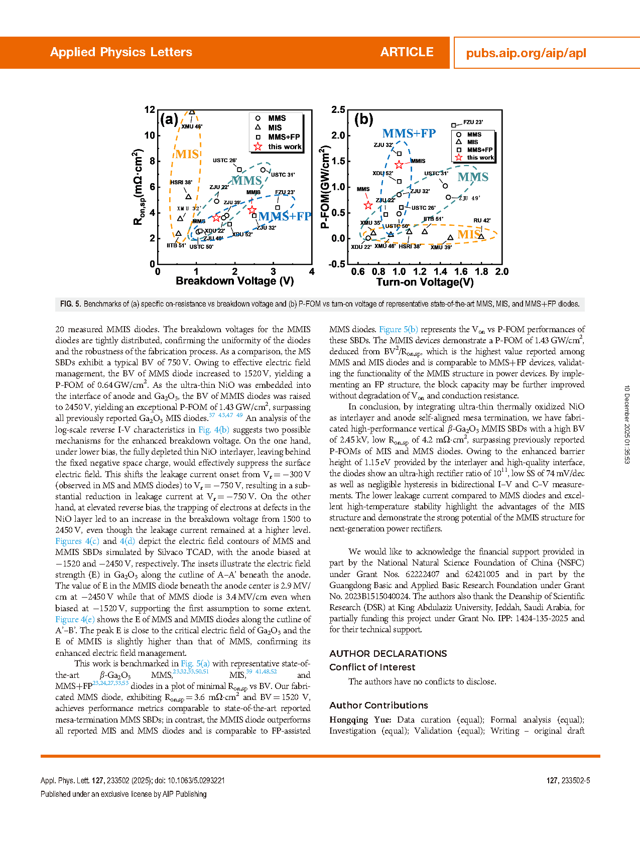
FIG. 5. Benchmarks of (a) specific on-resistance vs breakdown voltage and (b) P-FOM vs turn-on voltage of representative state-of-the-art MMS, MIS, and MMS+FP diodes.
DOI:
doi.org/10.1063/5.0293221