


Member News
【Member News】Debut at APCSCRM 2025: A Showcase of Jingsheng Electronics Technology’s Achievements and Gallium Oxide Products
日期:2025-12-15阅读:652
At the 6th Asia Pacific Conference on Silicon Carbide and Related Materials (APCSCRM 2025), Gallium Oxide emerged as one of the most prominent focal points in the field. As an invited participant, the Asian Gallium Oxide Alliance (AGOA) conducted an interview with its council member—Shandong Jingsheng Electronics Technology Co., Ltd.—during the conference. In the following section, we take a closer look at Raphael Optech, its core businesses, and its flagship products as presented.
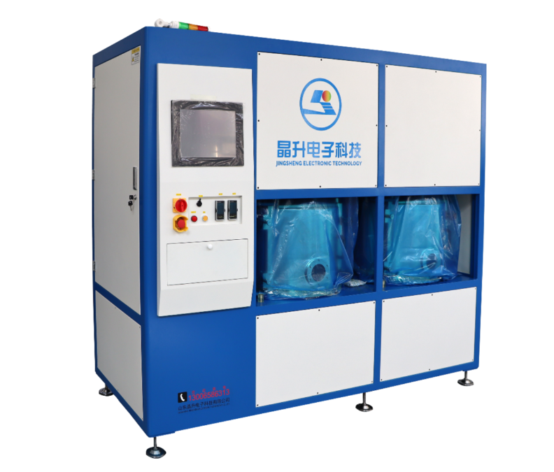
Shandong Jingsheng Electronics Technology Co., Ltd. is a national high-tech enterprise specializing in the R&D and manufacturing of semiconductor equipment. The company successfully completed intellectual property standardization in 2019, was recognized as a science and technology-based SME in Jinan, named a National High-Tech Enterprise in 2021, and in 2022 passed the GB/T9001-2016 Quality Management System certification. In 2023, it became a new member of the China Electronic Materials Industry Association, and in 2024 was recognized as a “Specialized, Refined, Distinctive, and Innovative” enterprise in Shandong Province and a “Gazelle Enterprise” in the same year.
The company’s main products include advanced equipment for third- and fourth-generation semiconductors and various crystal growth systems, widely applied in integrated circuit power devices, semiconductor materials, solar cells, LED chip manufacturing, new energy, and other fields. Jingsheng Electronics emphasizes technological innovation, holding multiple independent intellectual property rights, and is committed to providing customers with high-quality products and solutions. The company follows the business philosophy of “Integrity, Innovation, Cooperation, and Win-Win,” continuously enhancing core competitiveness and driving technological progress in the industry.
On November 27, 2025, the company officially put its newly expanded, standardized factory into operation, which not only expands production space and optimizes workflow but also injects strong momentum into product quality and delivery efficiency.
Main Products
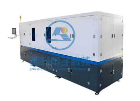
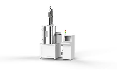
★ PVT Crystal Growth Furnace

1.Suitable for 6/8/12-inch conductive/high-purity semi-insulating SiC crystal growth.
2.Designed for long-duration, high-quality, large-scale crystal growth.
3.High-precision temperature and pressure control, excellent process performance, equipment consistency, with extensive mass production experience.
4.Optional constant power, constant current, or constant temperature operation modes.
5.One-key intelligent startup to reduce manual intervention and support scalable production.
6.Compact, vertical design for convenient layout and improved factory space utilization.
7.Equipped with high-precision butterfly valves and mass flow meters to control growth pressure, providing a stable crystal growth atmosphere with pressure control precision up to ±1 Pa.
★ HVPE Crystal Furnace (Gallium Oxide)
1.High growth rate, low defect density.
2.High lateral-to-vertical growth ratio, minimal porosity, capable of producing large-area thick films.
3.Single-crystal growth rate: ≥100 μm/hour.
4.Product sizes: 2/4/6 inches.
★ HVPE Vapor Phase Epitaxy Furnace (Gallium Oxide)
1.High growth rate, low defect density.
2.High lateral-to-vertical growth ratio, minimal porosity, enabling large-area thick film growth.
3.Epitaxial growth rate: ≥20 μm/hour.
4.Homogeneous Gallium Oxide epitaxial layer thickness: >10 μm.
5.Epitaxial wafer sizes: 2/4/6 inches.
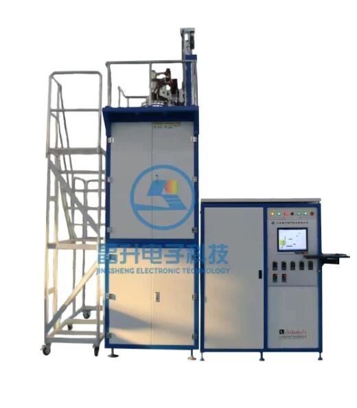
★ Resistance Crystal Furnace
1.Compact structure, can be arranged side by side to optimize factory space.
2.Compatible with resistive or induction heating.
3.Multiple heaters can be independently controlled; large process adjustment window for axial and radial temperature gradient control.
4.Bottom water-cooled crucible shaft with hollow temperature measurement holes; top, bottom, and sides equipped with infrared temperature measurement for process monitoring.
5.Optional constant power, constant current, or constant temperature operation modes.
6.Supports 6-8 inch semi-insulating/conductive crystal growth.
★ EFG (Edge-defined Film-fed Growth) Crystal Furnace
1.Designed for EFG pulling growth of ultra-wide bandgap single-crystal semiconductor materials.
2.Uses high-frequency heating and specialized thermal field design.
3.Supports 2-6 inch single-crystal growth, with customizable designs according to user requirements.
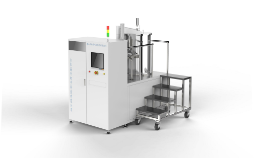
★ Seed Crystal Bonding Equipment
Application: Suitable for bonding seed crystals before SiC, GaN, and AlN growth, also applicable in the preparation and processing of the above crystals.
Features:
1.Seed crystals remain firmly attached at 2300°C.
2.100% bubble-free bonding.
3.High flatness.
4.Clean wafer surface, free of impurities.
Contact for more information:
Sales Phone: 13006586313 / 18375417816
Email: shandongjingsheng@126.com
Website: http://sdjsdz.com
Address: Building 10, International Enterprise Port, No. 2222 Yuqing Road, Ping’an Street, Changqing District, Jinan City, Shandong Province, China
