Paper Sharing
【Domestic Papers】Irradiation-Tolerant Diamond/ε-Ga₂O₃ Heterojunction Diode with Spatially Confined Leakage Failure and Ultrahigh Single-Event Burnout Voltage
日期:2025-12-15阅读:523
Researchers from the Ningbo Institute of Materials Technology and Engineering, Chinese Academy of Sciences have published a dissertation titled "Irradiation-Tolerant Diamond/ε-Ga2O3 Heterojunction Diode with Spatially Confined Leakage Failure and Ultrahigh Single-Event Burnout Voltage" in Materials Today Physics.
Project Support
This research was supported by National Natural Science Foundation of China (Grant No. 62204244), Fund of National Key Laboratory of Plasma Physics (6142A04240204), Ningbo Yongjiang Talent Introduction Programme (2021A-046-C). The authors would like to thank the Space Environment Simulation Research Infrastructure (SESRI) at Harbin Institute of Technology (HIT) for providing the heavy ion irradiation experiments.
Background
In strong-radiation environments such as space, high-energy particles can induce single-event effects (SEE) in semiconductor devices, leading to leakage, breakdown, and even catastrophic failure. As a result, the radiation tolerance of devices has become a key metric for high-reliability power electronics. Ultrawide-bandgap (UWBG) semiconductors such as Ga₂O₃ and diamond—owing to their ultra-large bandgap, high critical electric field, strong atomic bonds, and high displacement threshold energy—are regarded as an ideal material combination for constructing high-power, radiation-hardened devices. Although n-type Ga₂O₃ / p-type diamond heterojunction diodes have demonstrated high breakdown voltages and excellent thermal stability, existing wide-bandgap devices still commonly suffer from severe leakage current and SEB failure under heavy-ion irradiation, with SEB tolerance voltages typically below 600 V. Moreover, heavy-ion irradiation studies on diamond power devices remain very limited. Therefore, a systematic assessment of diamond/Ga₂O₃ heterostructures under extreme irradiation conditions is urgently needed to verify their potential to achieve high-voltage blocking and failure immunity in high-energy particle environments.
Abstract
Developing kilovoltage-class power devices with sufficient irradiation hardness is highly desired for aerospace application. However, the progress remains rather limited despite extensive research efforts devoted to screening various wide bandgap semiconductors and sophisticated device structures. Here, we demonstrate the use of a diamond/ε-Ga2O3 pn heterojunction to achieve robust irradiation tolerance exhibiting an ultrahigh single-event burnout (SEB) voltage over 1200 V under heavy ion irradiation with a linear energy transfer (LET) value of 82.1 MeV·cm2/mg. After the most severe irradiation experiment, the heterojunction diode exhibits slight increase of the leakage behavior rather than more catastrophic breakdown met in other devices. Microscopic analysis reveals that such behavior stems from a highly localized burnout region featuring the removal of the ε-Ga2O3 film and neighboring phase transition in the cathode edge. These results demonstrate the great potential of the heterostructure design based on ultrawide bandgap semiconductors for irradiation power application.
Conclusion
This work demonstrates a diamond/ε-Ga2O3 heterojunction diode exhibiting exceptional kilovolt-class VSEB and minimal localized irradiation damage after severe heavy ion irradiation with LETs up to 82.1 MeV·cm2/mg. The irradiated HJD maintains stable performance with merely a slight increase in leakage current, avoiding the catastrophic failure commonly observed in majority of diodes. With inherent resistance to irradiation-induced defect formation in ultrawide bandgap semiconductors, the combination of a p-type lightly doped diamond substrate with a moderately doped n-type ε-Ga2O3 thin film promotes the device irradiation tolerance by leveraging electric field crowding and transient thermal accumulation that usually amplifies the single-event burnout effect. Microstructural analysis combined with TCAD simulations confirms a highly localized burnout region near the cathode edge, characterized by limited removal of the ε-Ga2O3 layer and minor phase transformation. These findings underscore the potential of ultrawide-bandgap heterostructures for enabling high-voltage, irradiation-hardened power electronics suitable for critical aerospace applications.
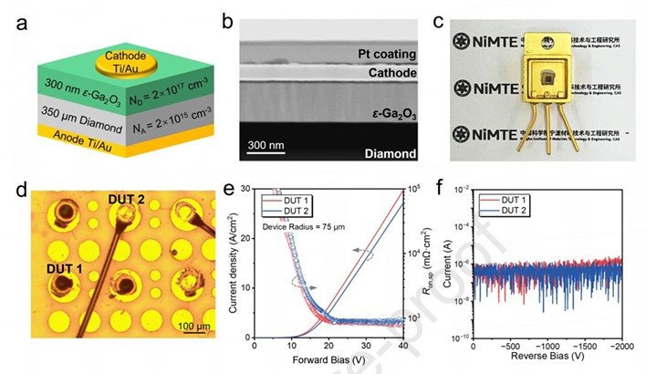
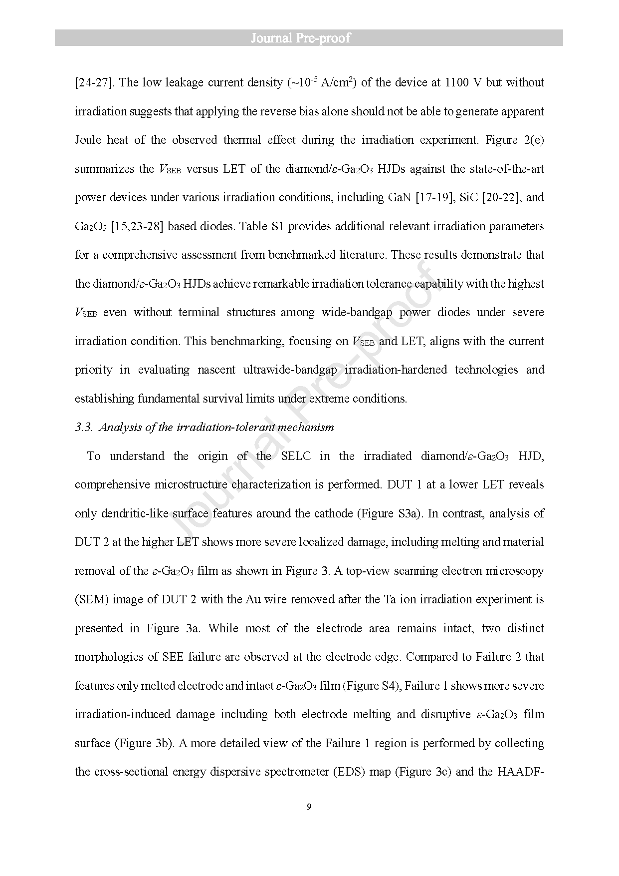
Figure 1. (a) Schematic of the diamond/ε-Ga2O3 HJD structure. (b) The cross-sectional low magnification STEM image of the HJD. Optical micrographs of (c) the packaged diode and (d) bonding spots with electrode radii of 75 μm (randomly selected as DUT 1 and 2). (e) Vertical current density and Ron,sp-voltage characteristics of DUT 1 and 2, respectively, exhibiting uniformity device performance. (f) Reverse current-voltage characteristics of DUT 1 and 2 before irradiation.
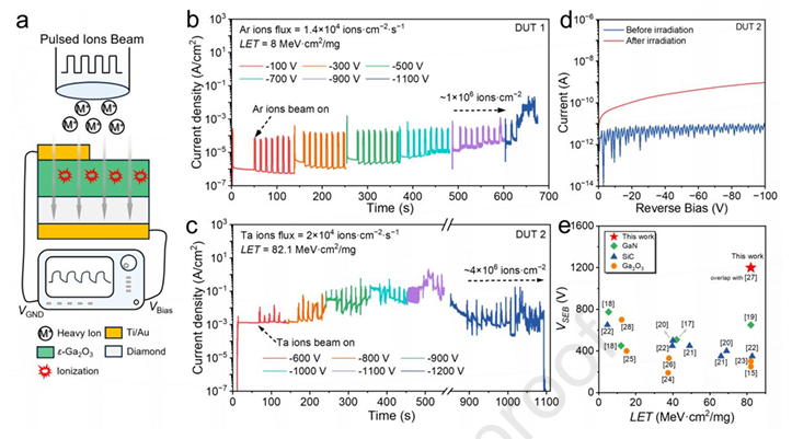
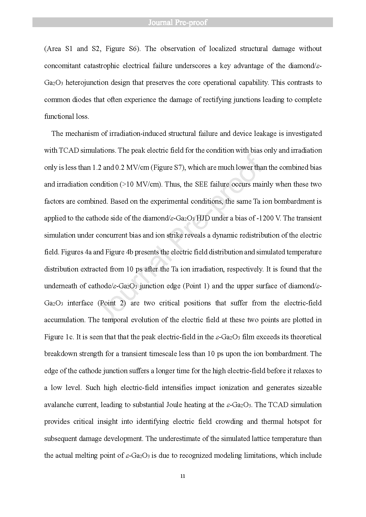
Figure 2. (a) Schematic of the heavy ion irradiation measurement of the diamond/ε-Ga2O3 HJD under various reverse voltages. Current-time characteristics at different reverse voltages of the diamond/ε-Ga2O3 DUTs under LET of (b) 8 and (c) 82.1 MeV·cm2/mg. (d) The reverse leakage current under bias voltages from 0 V to -100 V before and after Ta ion irradiation experiment. (e) Performance comparison of VSEB versus LET of representative GaN, SiC and Ga2O3 based power diodes under different irradiation conditions.

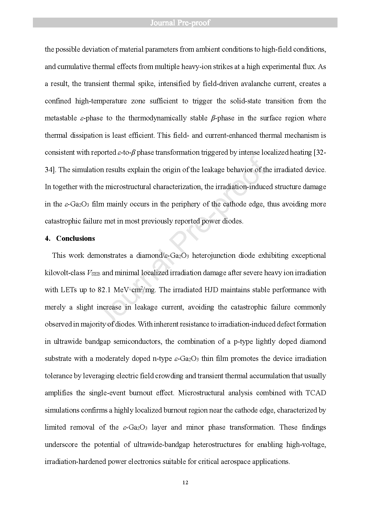
Figure 3. (a) The SEM image of DUT 2 showing representative ion-induced failure regions after the heavy ion irradiation measurement. The false yellow region highlights the Ti/Au electrode coverage over the ε-Ga2O3 film surface. (b) The magnified image of the major failure region 1 from (a). (c) EDS and (d) STEM images of the cross-section along the line shown in (b). (e)-(f) Cross-sectional TEM images of three representative failure characteristics extracted from respectively from Area 1, 2 and 3 in (d). High-resolution TEM images with insets of FFT patterns of (h) diamond, (i) ε-Ga2O3 and (j) phase-transformed region of β-Ga2O3, corresponding to the dashed rectangles in (g).
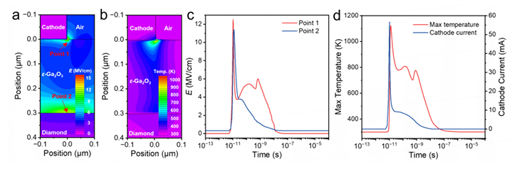
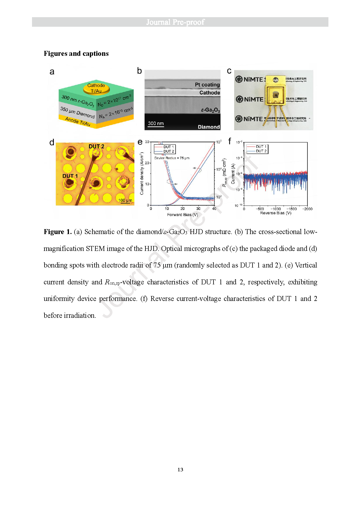
Figure 4. (a) Simulated electric-field and (b) temperature distribution of the diamond/ε-Ga2O3 HJD at the time scale of 10-11 s after a Ta ion striking under an anode voltage of -1200 V. The cathode/ε-Ga2O3 junction spot (Point 1) and the underlying diamond/ε-Ga2O3 spot (Point 2) are identified as two representative critical positions that suffer from electrical field accumulation and transient temperature uprise. (c) The corresponding time-resolved electric-field strength at Points 1 and 2 in (a) throughout a complete ion striking period. (d) The time-resolved maximum temperature and cathode current inside the device throughout the striking period.
DOI:
doi.org/10.1016/j.mtphys.2025.101942