


Member News
【Member News】Gallium Oxide Substrate Cost Slashed by 90%! DG Method Revolutionizes Crystal Growth as NCT and NEDO Drive Industry Transformation
日期:2025-12-22阅读:726
Novel Crystal Technology, Inc. which is engaged in the New Energy and Industrial Technology Development Organization (NEDO)’s “Key and Advanced Technology R&D through Cross Community Collaboration Program / Development of Material Technology for High-Quality and High-Efficiency Power Devices / High-Frequency Devices / Development of β-Ga2O3 wafers, power devices and power modules” (hereinafter referred to as the “Project”) has succeeded in developing a crystal growth method that does not use a crucible made of precious metals. This method is named Drop-fed Growth (DG) because of the feature of supplying raw material melt in droplets.
The DG method can significantly reduce the use of iridium, a very expensive precious metal, compared with the conventional Edge-defined Film-fed Growth (EFG) method. It may reduce the cost of manufacturing gallium oxide (β-Ga2O3) substrates to one-tenth that of the conventional method.
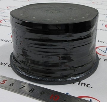
Figure 1. Crystal grown using the newly developed DG method
1. Background
β-Ga2O3*1 has excellent material properties for the manufacture of low-loss power devices*2 in medium-voltage (several hundred volts) market applications such as home appliances and electric vehicles, as well as power electronics equipment in high-voltage (several kilovolts) applications such as railways and power grids. For this reason, several large-budget national projects related to β-Ga2O3 have been undertaken domestically and internationally, and materials and device development are being carried out at a rapid pace.
Novel Crystal Technology, Inc. has been manufacturing β-Ga2O3 substrates using the EFG method since 2015. However, since the melting point of the raw material is as high as about 1800°C, the EFG method requires the use of a large amount of iridium, a very expensive precious metal that can withstand high temperatures, in the crucible that serves as the raw material container. As a way to reduce costs, we have been working on the development of a unique β-Ga2O3 crystal growth method that does not use iridium crucibles since FY2024.
2. Results of this project
By devising methods of heating and raw material supply, we succeeded in growing 95-mm-diameter β-Ga2O3 crystals without using iridium crucibles.
By heating the metal cylinder applying induction heating*3 to increase the temperature in the heating chamber, the surface of the crystal (seed crystal) is heated and melted by radiation from the aperture of the heating chamber. The aperture’s shape makes it easy to control the temperature distribution of the crystal’s surface in accordance with its diameter, allowing for larger diameters to be used. In addition, by continuously supplying raw material melt to the crystal surface in the form of droplets and pulling down the crystals, crystals can be grown without the use of iridium crucibles (Fig. 2).
The advantages of the developed DG method are as follows.
・The amount of iridium can be greatly reduced since no crucibles made of precious metals are
used.
・It is easy to make large-diameter crystals because of heating and melting of the crystal growth surface.
・Continuous supply of raw materials enables production of long crystals.
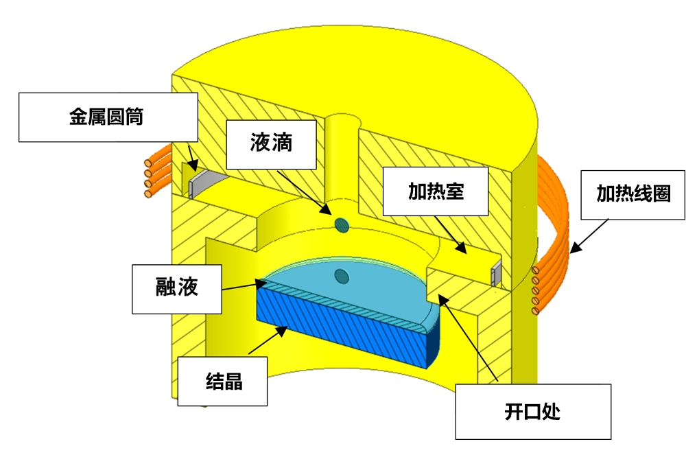
Fig. 2 Image of crystal growth equipment
Figure 3 shows a 95-mm-diameter β-Ga2O3 crystal grown by the DG method. The A part is the seed crystal, and the B part above it is the grown crystal. The crystal is cylindrical in shape, and the length of crystal growth is 50 mm. Impurities are added to form n-type crystals. β-Ga2O3 crystals become blue when only n-type impurities are added. The B part is dark blue, indicating that it is an n-type crystal.
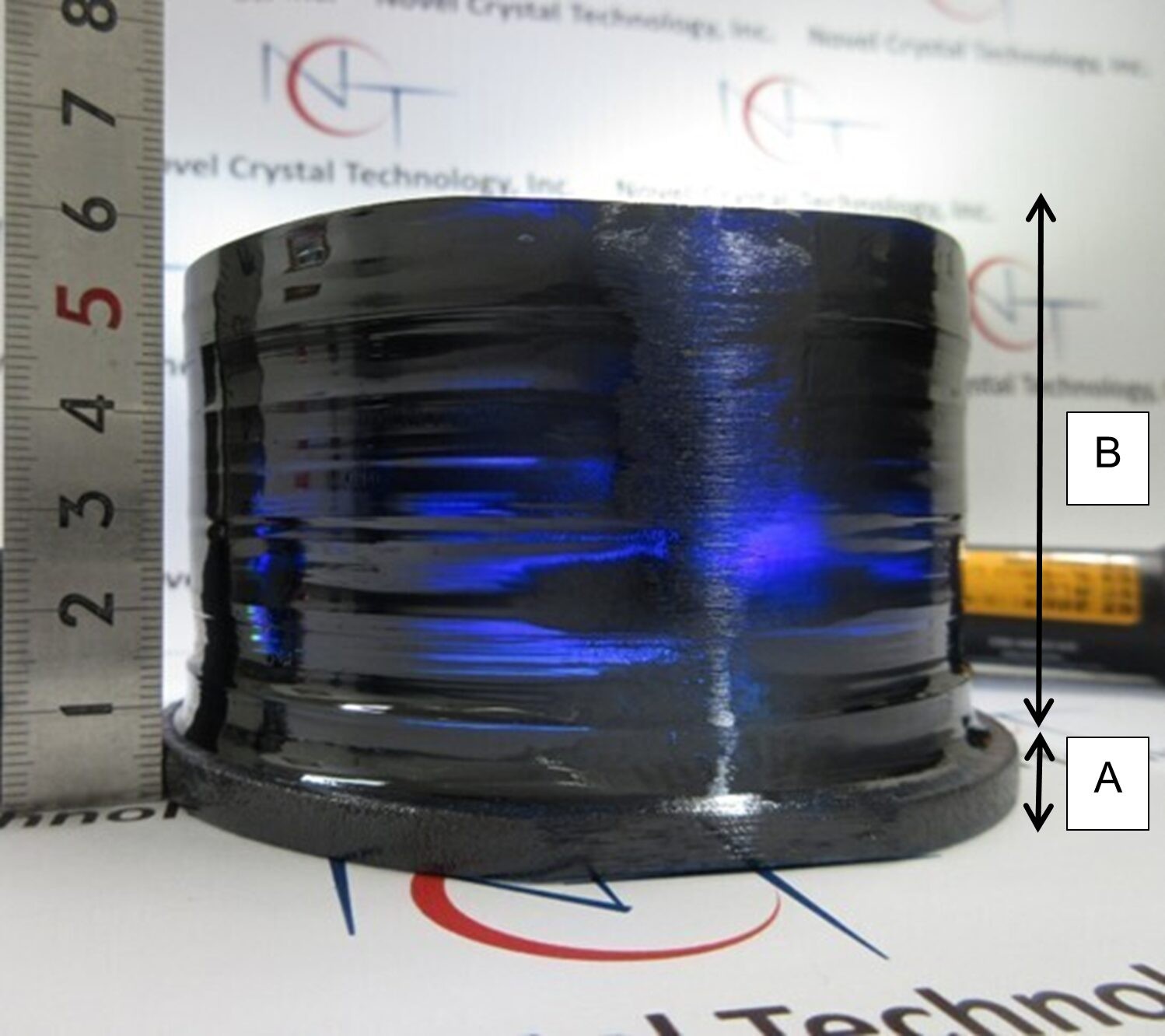
Fig. 3 A crystal grown by the DG method
(The A part is the seed crystal, and the B part indicates growth length)
It is estimated that the DG method can reduce the production cost of β-Ga2O substrates to one-tenth compared with the conventional EFG method by significantly reducing the amount of iridium used.
Patents on the DG method have been applied for in Japan and overseas, with the acquisition of rights currently underway.
・Japan: Patent No. 7633637 (Registered), Unexamined Patent Application Publication 2025-061932 (under
examination)
・United States: US 11,725,299 B2 (registered), US 12,163,246 B2 (registered)
・Europe: EP 3 945 147 A1 (under examination)
・China: CN 114000188 A (under examination)
3. Future plans
Novel Crystal Technology, Inc. is working on increasing the diameter and quality of the crystals grown in the DG method, and plans to ship 150-mm (6-inch) substrates in 2029 and 200-mm (8-inch) substrates in 2035.
[Note]
※1 β-Ga2O3
It is a compound of gallium and oxygen and is one of the wide-gap semiconductors.
※2 Power devices
Semiconductor devices have high breakdown voltages and can generate large currents, and are used in power
conversion equipment such as inverters.
※3 Induction heating
In crystal growth, a magnetic field created by passing high-frequency current through a coil is used to generate
eddy current in a metallic crucible installed inside the coil and heat it.
4. For more information, please contact
First Research Department, Novel Crystal Technology Tel: +81-4-2900-0072
Learn more/WENDER-SINO
Novel Crystal Technology, Inc. (NCT), Japan, is the world’s first company engaged in the research, development, and production of Gallium Oxide substrates, epitaxy, and devices. As the pioneer in the global Gallium Oxide field, NCT integrates substrate manufacturing, epitaxial growth, and device R&D and production. From crystal growth and substrate fabrication to epitaxy and device development, NCT remains at the forefront of the global Gallium Oxide industry, driving the industrialization of Gallium Oxide technologies.
Wonder-Sino Group, as NCT’s designated agent in China, is fully responsible for brand marketing, market promotion, and after-sales services for NCT in the Chinese region. Adhering to the core philosophy of “leading-edge technologies and customer-oriented service,” the company leverages world-class advanced technologies to deliver deeply customized, integrated solutions combining materials + equipment + process, creating irreplaceable industrial value for customers.
NCT continues to focus deeply on Gallium Oxide, a core material in the fourth-generation ultrawide-bandgap semiconductor field, advancing the full industrial chain—from substrates to epitaxy and devices—while driving technological innovation across the industry. Currently, NCT’s full range of Gallium Oxide products has passed rigorous verification by major global research institutions and leading enterprises, with related reports published. For more information, please visit the “News” section on the Wonder-Sino website (www.wonder-sino.com).
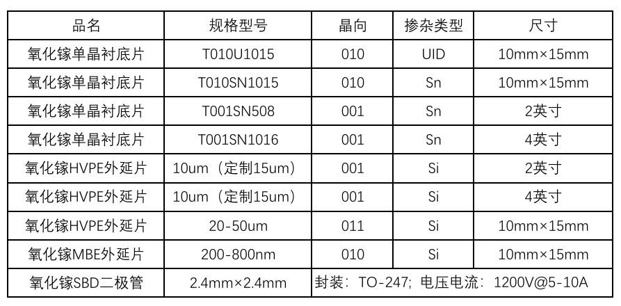
Related product specifications are provided below:
Looking ahead, NCT will continue to increase investment in Gallium Oxide material research and is committed to providing higher-quality products for global customers. At the same time, NCT will work together with Wonder-Sino to explore the unlimited potential of Gallium Oxide materials and contribute to the innovative development of the global Gallium Oxide industry.
For further product information, please contact:
Contact Person: Ms. Guo – 13164023887
Email: gxm@wonder-sino.com
Website: www.wonder-sino.com
