Paper Sharing
【International Papers】Direct Probing of Trap Dynamics in β-Ga₂O₃ Schottky Barrier Diodes Using Single-Voltage-Pulse Characterization
日期:2025-12-30阅读:481
Researchers from the Korea Aerospace University have published a dissertation titled "Direct Probing of Trap Dynamics in β-Ga2O3 Schottky Barrier Diodes Using Single-Voltage-Pulse Characterization" in Advanced Science.
Background
Gallium oxide (β-Ga2O3) is a semiconductor material with an ultrawide bandgap (≈4.8 eV) and an exceptionally high theoretical breakdown electric field (≈8 MV cm−1). These unique properties make it a promising candidate for next-generation power electronics, solar-blind ultraviolet photodetectors, and devices designed for harsh environments. However, the presence of defect states within the bandgap often hinders the material from reaching its full potential. The origin of these defect states in β-Ga2O3 is complex and generally attributed to both intrinsic and extrinsic sources. Intrinsic defects, which arise from imperfections in the crystal lattice, include native point defects such as gallium vacancies (VGa), oxygen vacancies (VO), and their associated complexes.Extrinsic defects, on the other hand, originate from the unintentional incorporation of impurity atoms, such as silicon (Si) and iron (Fe), during high-temperature growth processes. These defects introduce localized energy levels within the bandgap that act as traps, capturing and emitting charge carriers. These traps can significantly impact device operation and reliability, including current collapse, threshold voltage instability, and degradation of switching characteristics. Therefore, a precise characterization and comprehensive understanding of these trap states are crucial for further advancing β-Ga2O3-based device technologies.
Abstract
Gallium oxide (β-Ga2O3) is a promising ultrawide-bandgap semiconductor for next-generation power electronics, but its performance is strongly limited by trap states that capture carriers. In this study, a single-pulse characterization method is presented to directly probe trap dynamics in β-Ga2O3 Schottky barrier diodes (SBDs). Transient current responses are systematically investigated under varying pulse widths, rise and fall times, amplitudes, and temperatures. The results reveal that traps in the neutral region progressively participate in electron capture, resulting in current decay during the constant-voltage phase. Additionally, a delayed trap response produces asymmetry between the ramp-up and ramp-down transients. Analysis of the current decay yielded a trap density of ≈5×1014 cm−2, representing the total trap density near the Schottky junction. Exponential fitting provides a carrier capture time constant of ≈ 30 µs at a forward bias of 2 V, consistent with the onset of trap-induced current degradation. Temperature-dependent measurements indicate that carrier capture is suppressed at elevated temperatures, resulting in a trap activation energy of ≈0.16 eV. These findings demonstrate that the single-pulse method offers a straightforward and effective approach for evaluating trap states under practical operating conditions in β-Ga2O3 devices.
Conclusion
This work demonstrates a single-pulse characterization method for directly probing trap dynamics in the β-Ga2O3 SBDs. By analyzing transient current responses under varied pulse widths, rise and fall times, amplitudes, and temperatures, we systematically extracted trap parameters and clarified their influence on carrier transport. The results reveal that traps in the neutral region progressively participate in electron capture, leading to current decay during the constant-voltage phase. This delayed trap response also accounts for the asymmetric behaviors observed during ramp-up and ramp-down. The extracted trapped carrier density, ≈5 × 1014 cm−2, represents the total trap density in the vicinity of the Schottky barrier junction. Furthermore, the carrier capture time constant was determined to be ≈30 µs at a forward bias of 2 V. Temperature-dependent measurements confirmed the suppression of carrier capture at elevated temperatures and yielded a trap activation energy of ≈0.16 eV, consistent with previously reported values. Overall, the proposed single-pulse technique offers a straightforward and effective means to evaluate trap states under conditions directly relevant to device operation, thereby enhancing the understanding of defect-related effects in β-Ga2O3 devices.
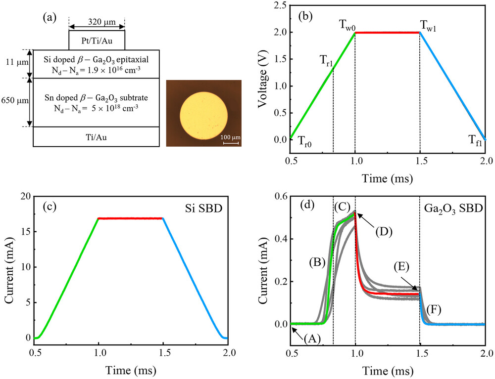
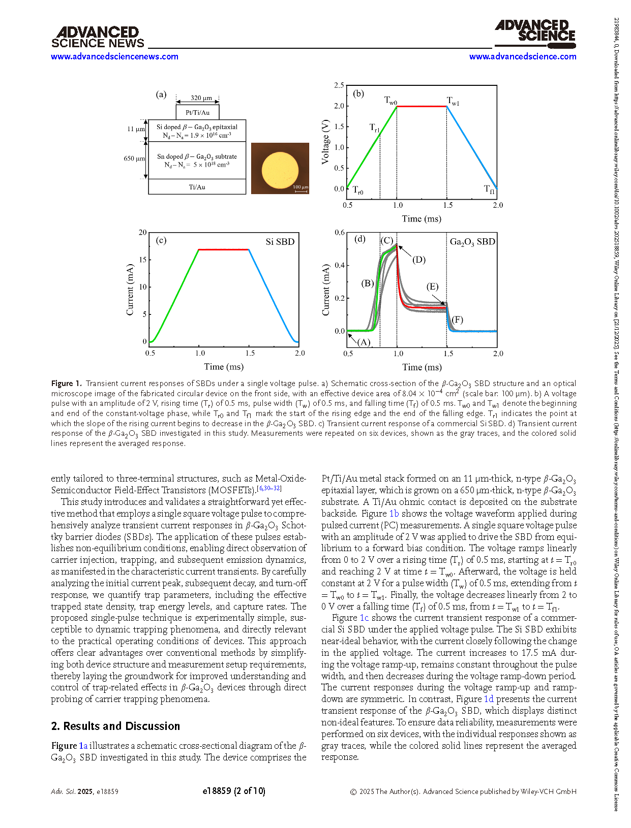
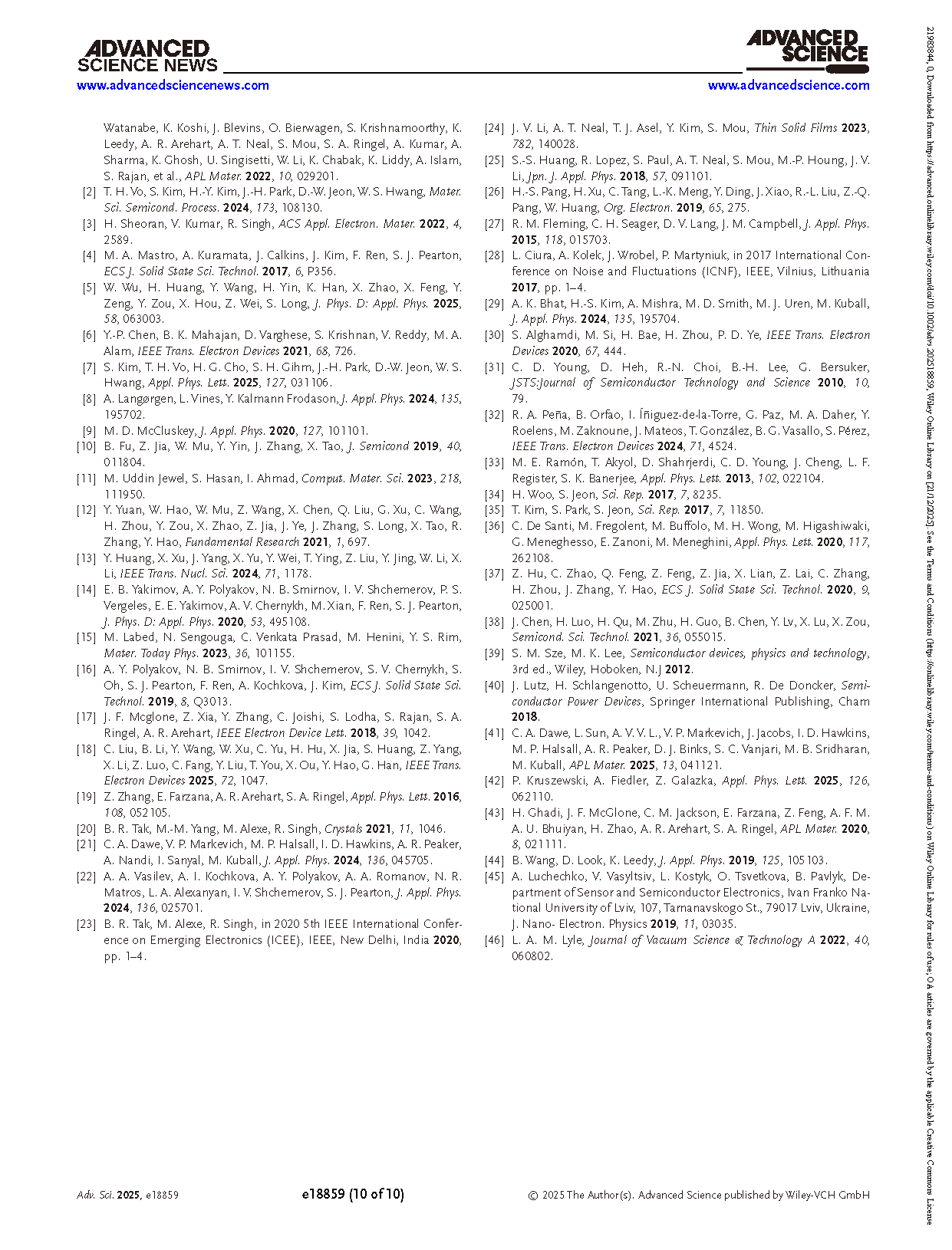
Figure 1. Transient current responses of SBDs under a single voltage pulse. a) Schematic cross-section of the β-Ga2O3 SBD structure and an optical microscope image of the fabricated circular device on the front side, with an effective device area of 8.04 × 10⁻⁴ cm2 (scale bar: 100 µm). b) A voltage pulse with an amplitude of 2 V, rising time (Tr) of 0.5 ms, pulse width (Tw) of 0.5 ms, and falling time (Tf) of 0.5 ms. Tw0 and Tw1 denote the beginning and end of the constant-voltage phase, while Tr0 and Tf1 mark the start of the rising edge and the end of the falling edge. Tr1 indicates the point at which the slope of the rising current begins to decrease in the β-Ga2O3 SBD. c) Transient current response of a commercial Si SBD. d) Transient current response of the β-Ga2O3 SBD investigated in this study. Measurements were repeated on six devices, shown as the gray traces, and the colored solid lines represent the averaged response.
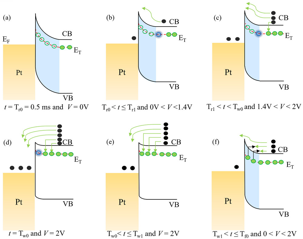
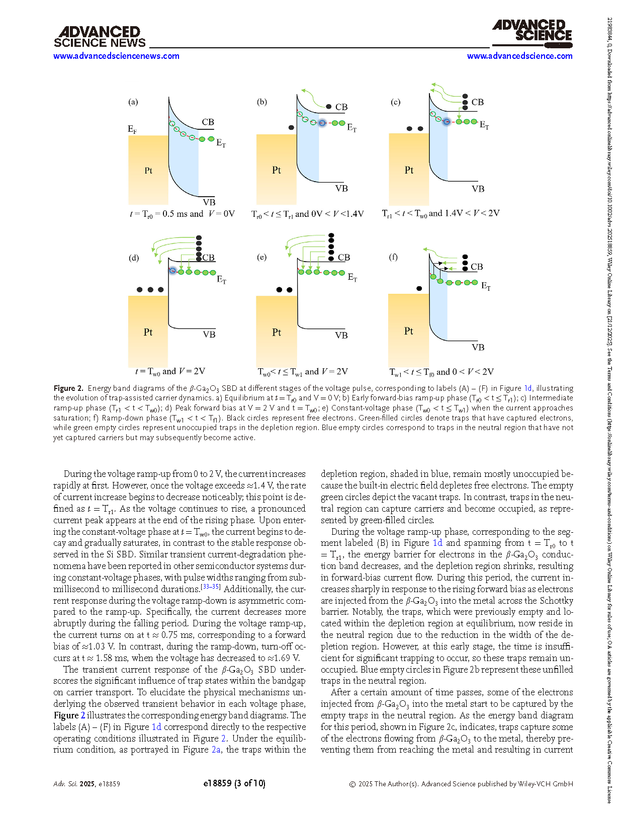
Figure 2. Energy band diagrams of the β-Ga2O3 SBD at different stages of the voltage pulse, corresponding to labels (A) – (F) in Figure 1d, illustrating the evolution of trap-assisted carrier dynamics. a) Equilibrium at t = Tr0 and V = 0 V; b) Early forward-bias ramp-up phase (Tr0 < t ≤ Tr1); c) Intermediate ramp-up phase (Tr1 < t < Tw0); d) Peak forward bias at V = 2 V and t = Tw0; e) Constant-voltage phase (Tw0 < t ≤ Tw1) when the current approaches saturation; f) Ramp-down phase (Tw1 < t < Tf1). Black circles represent free electrons. Green-filled circles denote traps that have captured electrons, while green empty circles represent unoccupied traps in the depletion region. Blue empty circles correspond to traps in the neutral region that have not yet captured carriers but may subsequently become active.
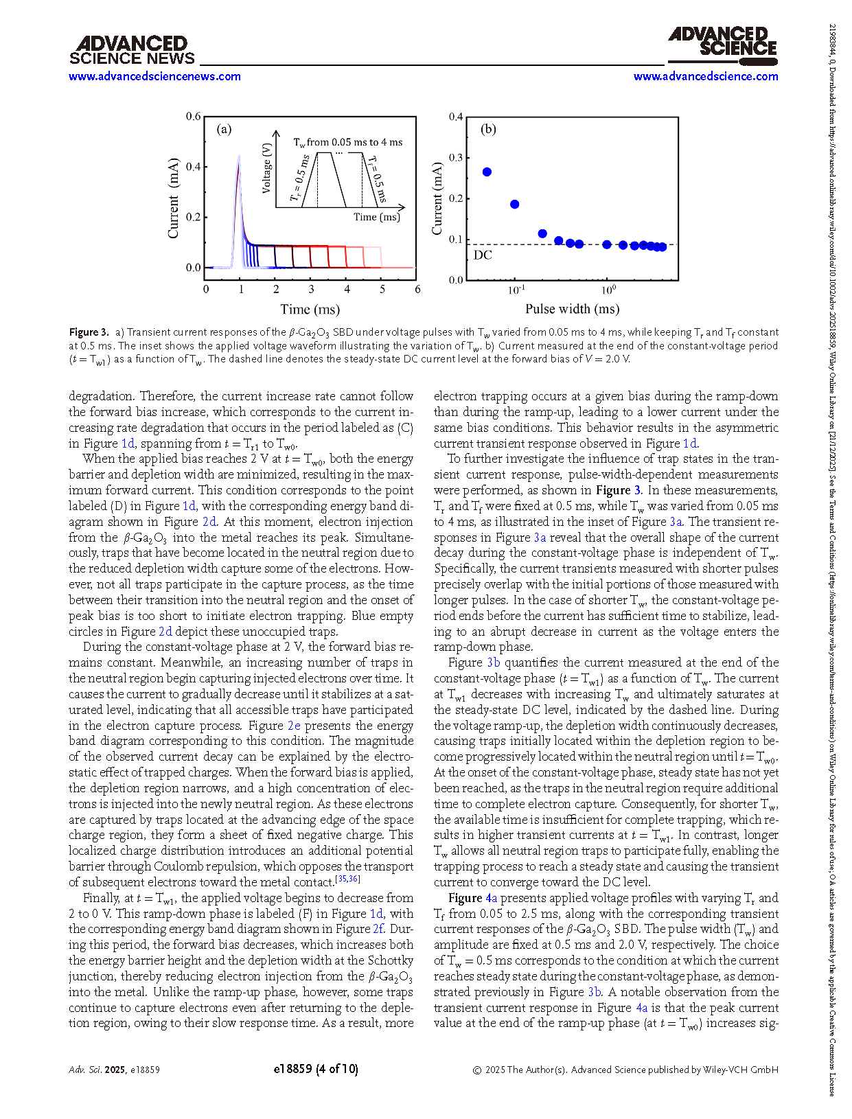
Figure 3. a) Transient current responses of the β-Ga2O3 SBD under voltage pulses with Tw varied from 0.05 ms to 4 ms, while keeping Tr and Tf constant at 0.5 ms. The inset shows the applied voltage waveform illustrating the variation of Tw. b) Current measured at the end of the constant-voltage period (t = Tw1) as a function of Tw. The dashed line denotes the steady-state DC current level at the forward bias of V = 2.0 V.
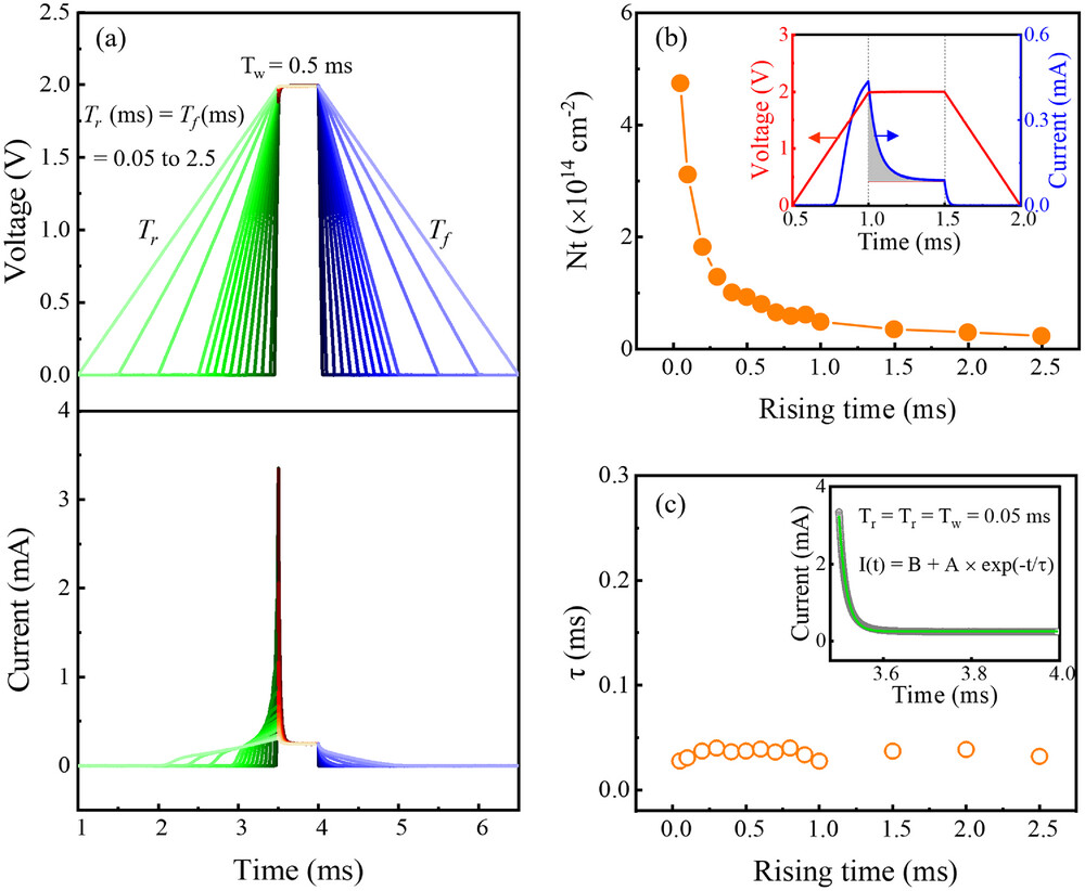
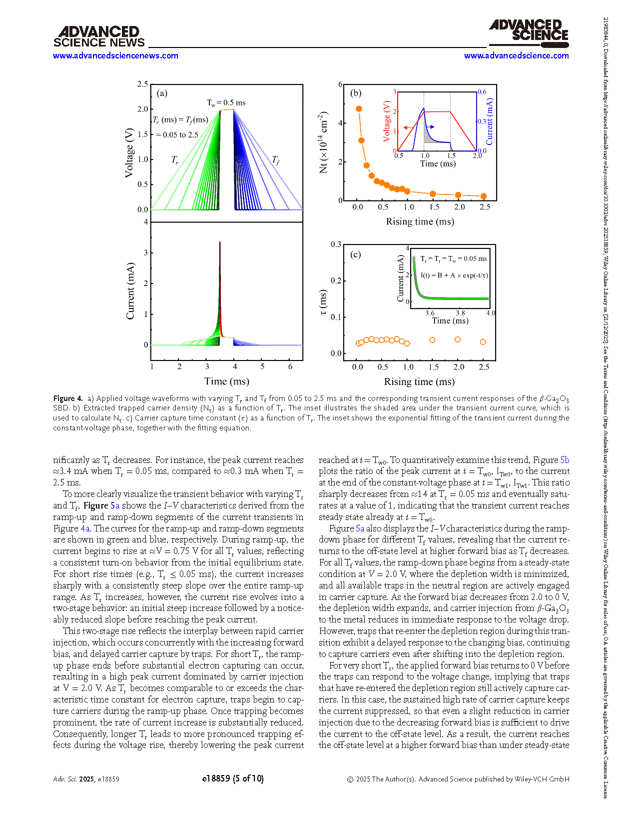
Figure 4. a) Applied voltage waveforms with varying Tr and Tf from 0.05 to 2.5 ms and the corresponding transient current responses of the β-Ga2O3 SBD. b) Extracted trapped carrier density (Nt) as a function of Tr. The inset illustrates the shaded area under the transient current curve, which is used to calculate Nt. c) Carrier capture time constant (τ) as a function of Tr. The inset shows the exponential fitting of the transient current during the constant-voltage phase, together with the fitting equation.
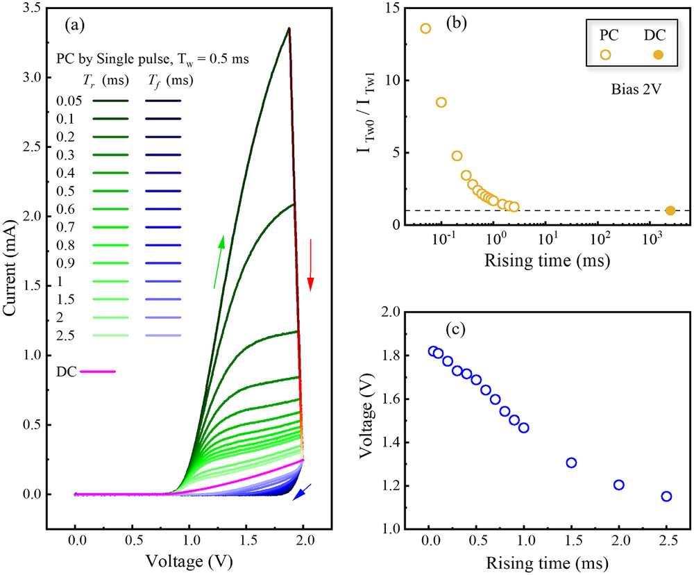
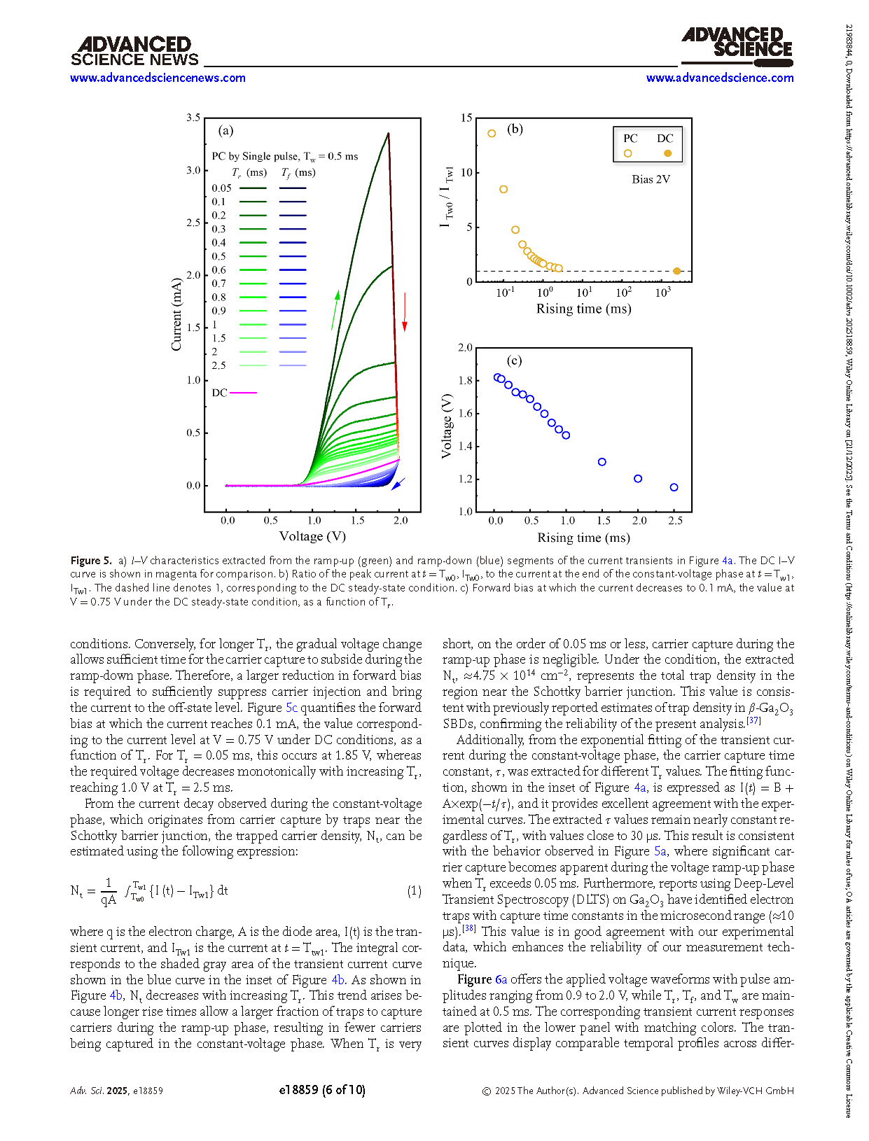
Figure 5. a) I–V characteristics extracted from the ramp-up (green) and ramp-down (blue) segments of the current transients in Figure 4a. The DC I–V curve is shown in magenta for comparison. b) Ratio of the peak current at t = Tw0, ITw0, to the current at the end of the constant-voltage phase at t = Tw1, ITw1. The dashed line denotes 1, corresponding to the DC steady-state condition. c) Forward bias at which the current decreases to 0.1 mA, the value at V = 0.75 V under the DC steady-state condition, as a function of Tr.
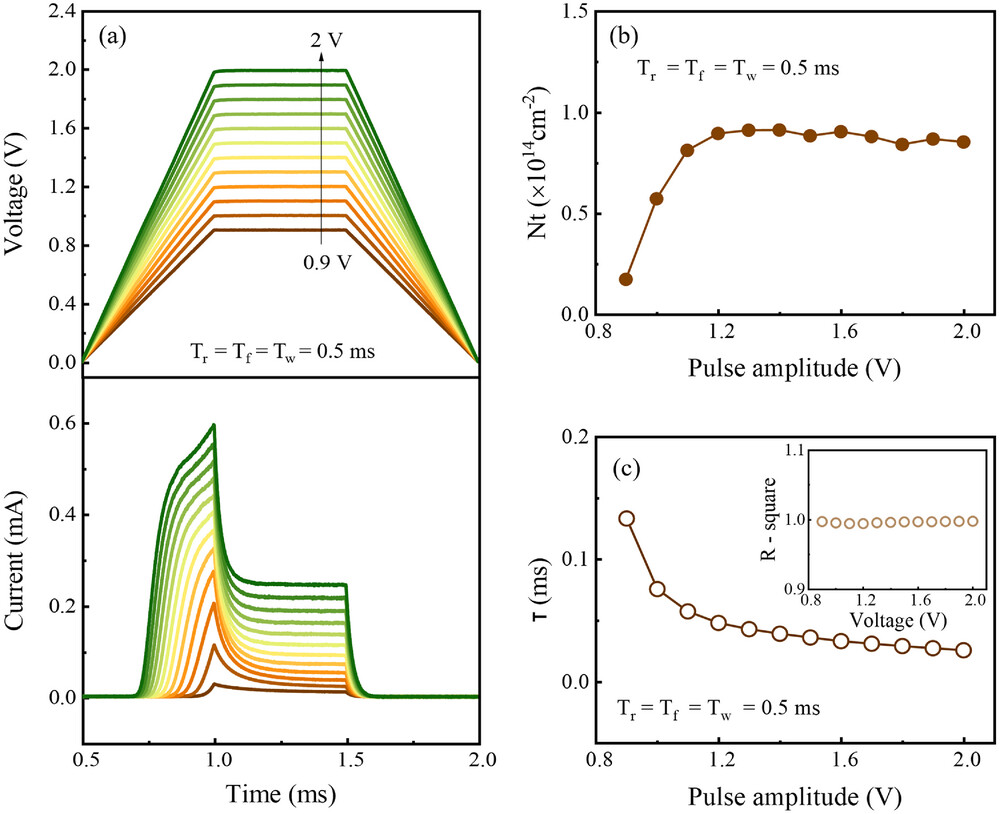
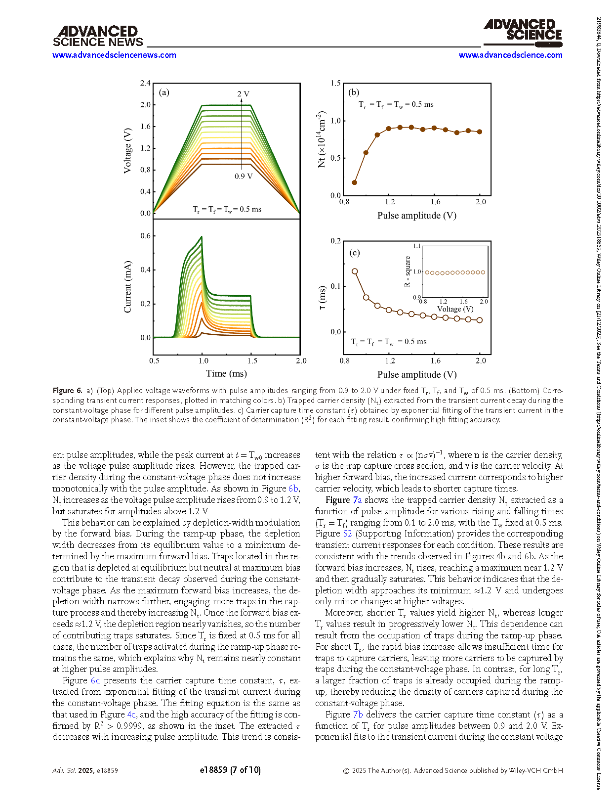
Figure 6. a) (Top) Applied voltage waveforms with pulse amplitudes ranging from 0.9 to 2.0 V under fixed Tr, Tf, and Tw of 0.5 ms. (Bottom) Corresponding transient current responses, plotted in matching colors. b) Trapped carrier density (Nt) extracted from the transient current decay during the constant-voltage phase for different pulse amplitudes. c) Carrier capture time constant (τ) obtained by exponential fitting of the transient current in the constant-voltage phase. The inset shows the coefficient of determination (R2) for each fitting result, confirming high fitting accuracy.
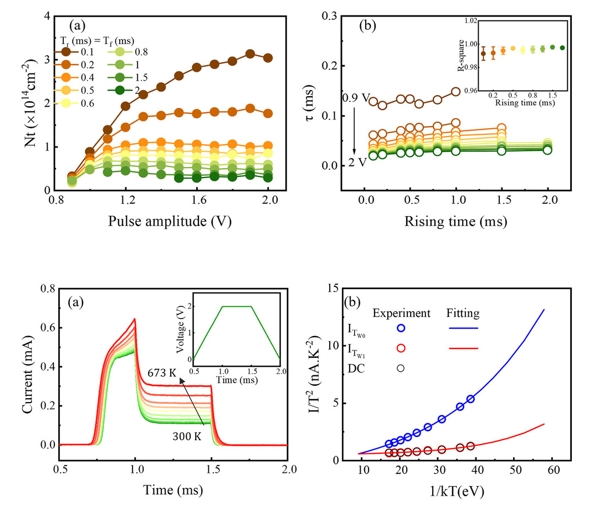
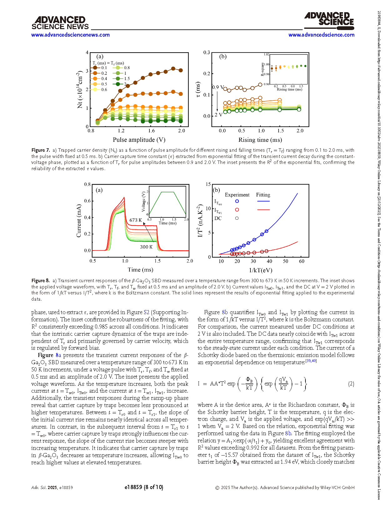
Figure 7. a) Trapped carrier density (Nt) as a function of pulse amplitude for different rising and falling times (Tr = Tf) ranging from 0.1 to 2.0 ms, with the pulse width fixed at 0.5 ms. b) Carrier capture time constant (τ) extracted from exponential fitting of the transient current decay during the constant-voltage phase, plotted as a function of Tr for pulse amplitudes between 0.9 and 2.0 V. The inset presents the R2 of the exponential fits, confirming the reliability of the extracted τ values.
DOI:
doi.org/10.1002/advs.202518859