Paper Sharing
【International Papers】κ-Ga₂O₃/(B)GaAs/GaAs Heterostructures: Study of Optically Active Defects, Design, and Modeling of Solar Cells Based on These Heterostructures
日期:2025-12-31阅读:449
Researchers from the ACS Omega have published a dissertation titled "κ-Ga2O3/(B)GaAs/GaAs Heterostructures: Study of Optically Active Defects, Design, and Modeling of Solar Cells Based on These Heterostructures" in ACS Omega.
Background
The global shift toward renewable energy has driven intense research into advanced photovoltaic (PV) technologies capable of outperforming traditional single-junction solar cells (SCs). Among the most promising approaches, there is the intermediate band solar cell (IBSC), a concept proposed to overcome the Shockley–Queisser limit by enabling the absorption of low-energy (sub-bandgap) photons via an intermediate energy level forming an intermediate band (IB) positioned within the host semiconductor bandgap. This IB allows for two-step photon absorption: from the valence band (VB) to the IB, and from the IB to the conduction band (CB), thereby enhancing photocurrent generation while preserving high output voltage. Hence, the realization of efficient IBSCs requires advanced material systems with engineered band structures and tailored optical and electronic properties. A particularly attractive platform to achieve IBs involves wide/narrow bandgap heterostructures. The IB formation might be achieved at the interface via quantum confinement, defect states, or impurity-induced band anticrossing effects. In this study, we present a detailed investigation of the emission characteristics of such heterostructures through temperature-dependent PL and e-beam-energy-dependent CL to highlight the defect-assisted and radiative recombination mechanisms. Furthermore, the device performance of Ga2O3/GaAs and Ga2O3/BGaAs/GaAs heterostructures is predicted, specifically looking at their application in IBSCs. Band alignment and energy level formation at the interfaces, quantum efficiency (QE), and J–V characteristics under standard AM1.5 illumination are simulated using SCAPS-1D. This work aims at establishing the experimental and theoretical bases for the fabrication of Ga2O3-based IBSC architectures and offers novel insights into the role of oxide/III–V interfaces and boron incorporation in enabling high-performance SCs.
Abstract
This work focuses on the steady-state luminescence of pure-phase κ-Ga2O3/GaAs and κ-Ga2O3/BGaAs/GaAs heterostructures grown by metal–organic chemical vapor deposition. The films were characterized by electron beam (e-beam) energy-dependent cathodoluminescence (CL) and steady-state photoluminescence (PL), supported by one-dimensional Solar Cell Capacitance Simulator (SCAPS-1D) simulation, to assess their possible application as intermediate energy band layers in solar cells. The power- and temperature-dependent PL and CL show that the luminescence in κ-Ga2O3/GaAs and κ-Ga2O3/a-BGaO/BGaAs/GaAs heterostructures, where a-BGaO represents a thin amorphous BGaO interlayer between the κ-Ga2O3 film and BGaAs template, is dominated by donor–acceptor transitions. These transitions originated from point defect ensembles tuned by the disorder at the interface, which give rise to the formation of minibands. The boron-to-gallium substitution, boron segregation, gallium diffusion, and point defects clustering at the interface are supposed to play a crucial role in the luminescence mechanisms. The heterojunction features are promising in view of the development of a new class of active layers in photodetectors working in the visible and infrared regions. We propose a novel solar cell structure in which the insertion of a BGaAs/a-BGaO interlayer between GaAs and κ-Ga2O3 may substantially enhance the solar cell parameters. The SCAPS-1D simulations suggest that the κ-Ga2O3/a-BGaO/BGaAs/GaAs heterostructure may reach a power conversion efficiency (PCE) of 23.76% with an open-circuit voltage (Voc) of 0.92 V, a short-circuit current density (Jsc) of 32.61 mA/cm2, and a fill factor (FF) of 78.66%.
Conclusion
κ-Ga2O3/GaAs and κ-Ga2O3/BGaAs/GaAs heterostructures, prepared by MOCVD, were characterized by PL and CL. Low-temperature PL measurements of κ-Ga2O3/GaAs structure evidenced a point defect-related luminescence, a broadening, and a red shift of the buried GaAs layer with respect to pristine GaAs. This is believed to be related to the diffusion of Ga atoms from the top κ-Ga2O3 layer into the GaAs substrate, which reduces the vacancy density and generates GaAs acceptors.
PL and CL measurements show that luminescence in buried GaAs is not of an excitonic nature and more likely dominated by donor-to-acceptor transitions related to VGa that form PDEs distributed in the bandgap. The observations made on κ-Ga2O3/GaAs are useful to understand the luminescence mechanisms in the κ-Ga2O3/BGaAs/GaAs heterostructure. In the latter case, the CL intensity is double in comparison to that of κ-Ga2O3/GaAs, with the emission tuned by PDEs forming band-tail states.
Based on the properties of the κ-Ga2O3/BGaAs/GaAs heterostructure, we proposed a SC prototype that includes this material stack. The simulation of the TCO/Ga2O3/BGaAs/GaAs/Au prototype suggests a total QE of ∼90%, six times higher than TCO/Ga2O3/GaAs/Au and a broadened response ranging from the deep UV to the infrared spectrum (200–1000 nm). The insertion of a BGaAs interlayer in the SC suggests a PCE of 23.76%, Voc of 0.92 V, Jsc of 32.61 mA/cm2, and an FF of 78.66%. This preliminary demonstration of the κ-Ga2O3/(B)GaAs/GaAs heterostructure is expected to pave the way to functional and physical integration of Ga2O3 with other materials. The fabrication of fully functional devices and their testing, including accelerated aging, thermal cycling, electrical characterization after prolonged illumination, and bias stress tests, combined with structural and compositional analyses, are necessary in order to quantify degradation mechanisms and confirm the long-term stability of the heterostructures.

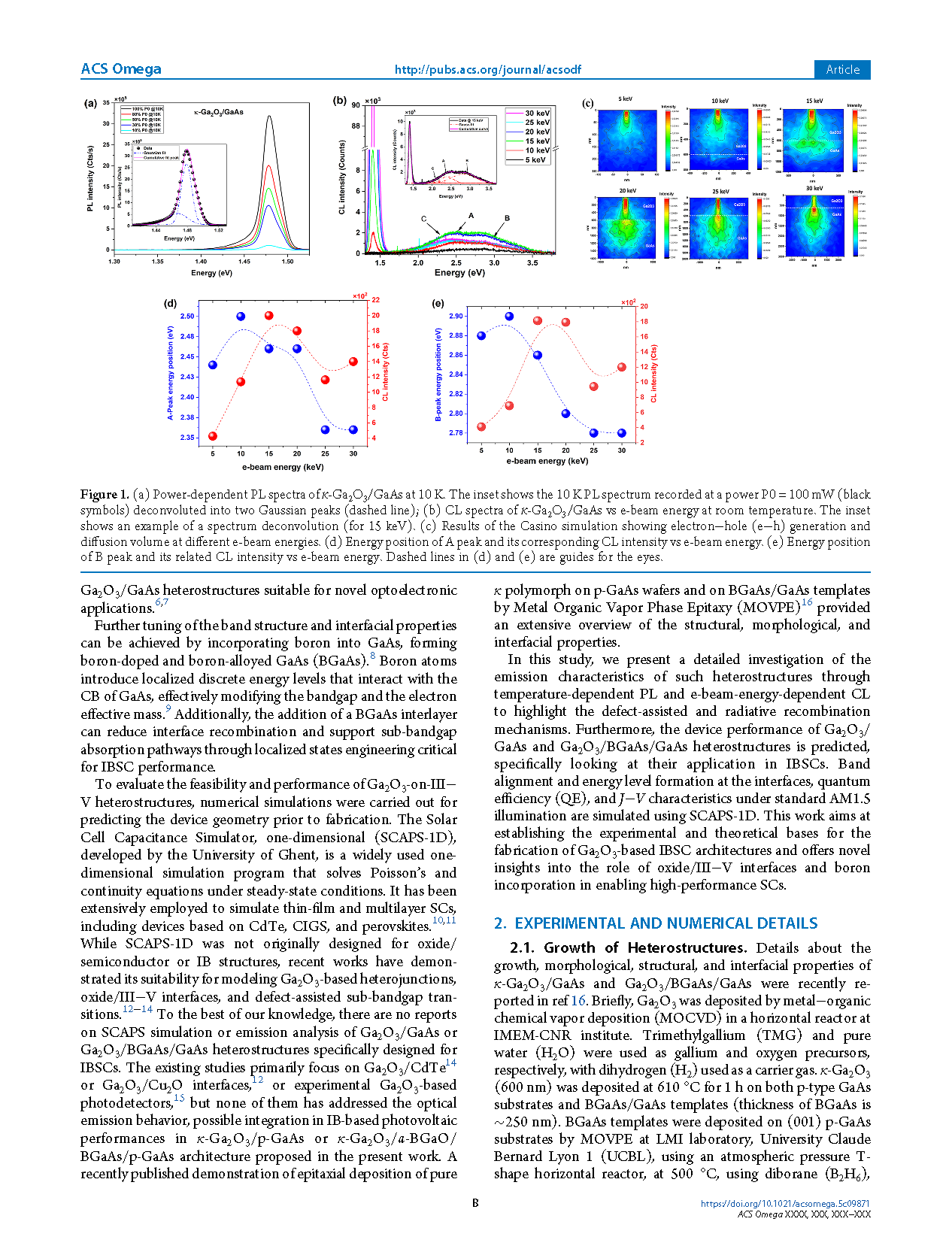
Figure 1. (a) Power-dependent PL spectra of κ-Ga2O3/GaAs at 10 K. The inset shows the 10 K PL spectrum recorded at a power P0 = 100 mW (black symbols) deconvoluted into two Gaussian peaks (dashed line); (b) CL spectra of κ-Ga2O3/GaAs vs e-beam energy at room temperature. The inset shows an example of a spectrum deconvolution (for 15 keV). (c) Results of the Casino simulation showing electron–hole (e–h) generation and diffusion volume at different e-beam energies. (d) Energy position of A peak and its corresponding CL intensity vs e-beam energy. (e) Energy position of B peak and its related CL intensity vs e-beam energy. Dashed lines in (d) and (e) are guides for the eyes.
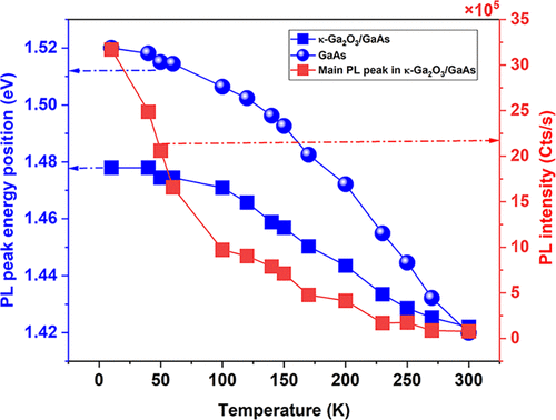
Figure 2. Temperature-dependent PL energy of the main emission peak of the undoped κ-Ga2O3/GaAs heterostructure (blue squares) and its corresponding intensity (red squares). The PL peak energy position of the GaAs reference substrate is also reported (blue balls). The excitation power is fixed at 100 mW for all temperatures.
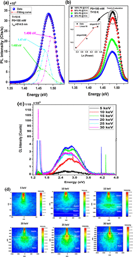
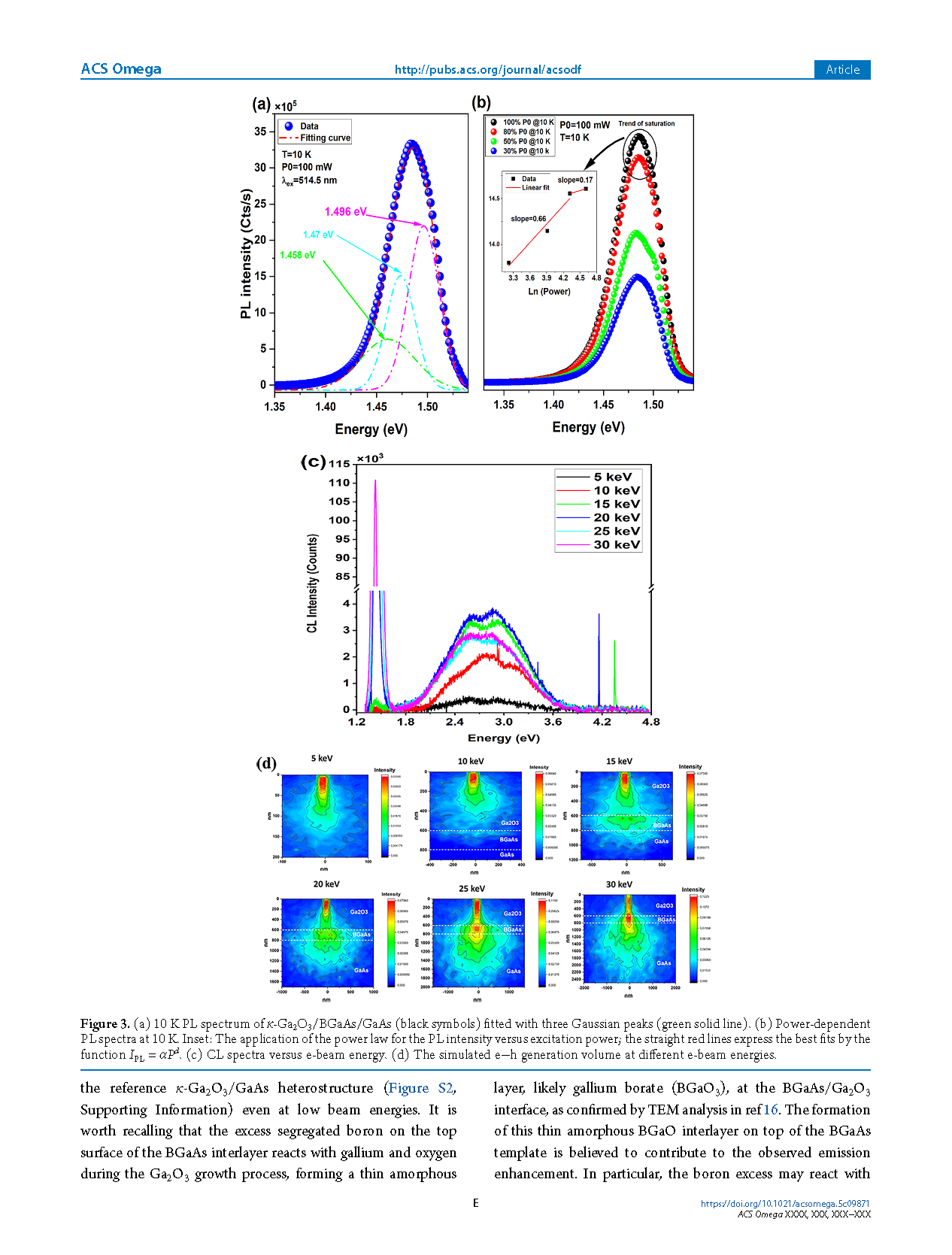
Figure 3. (a) 10 K PL spectrum of κ-Ga2O3/BGaAs/GaAs (black symbols) fitted with three Gaussian peaks (green solid line). (b) Power-dependent PL spectra at 10 K. Inset: The application of the power law for the PL intensity versus excitation power; the straight red lines express the best fits by the function IPL = αPd. (c) CL spectra versus e-beam energy. (d) The simulated e–h generation volume at different e-beam energies.
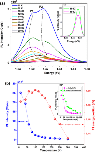
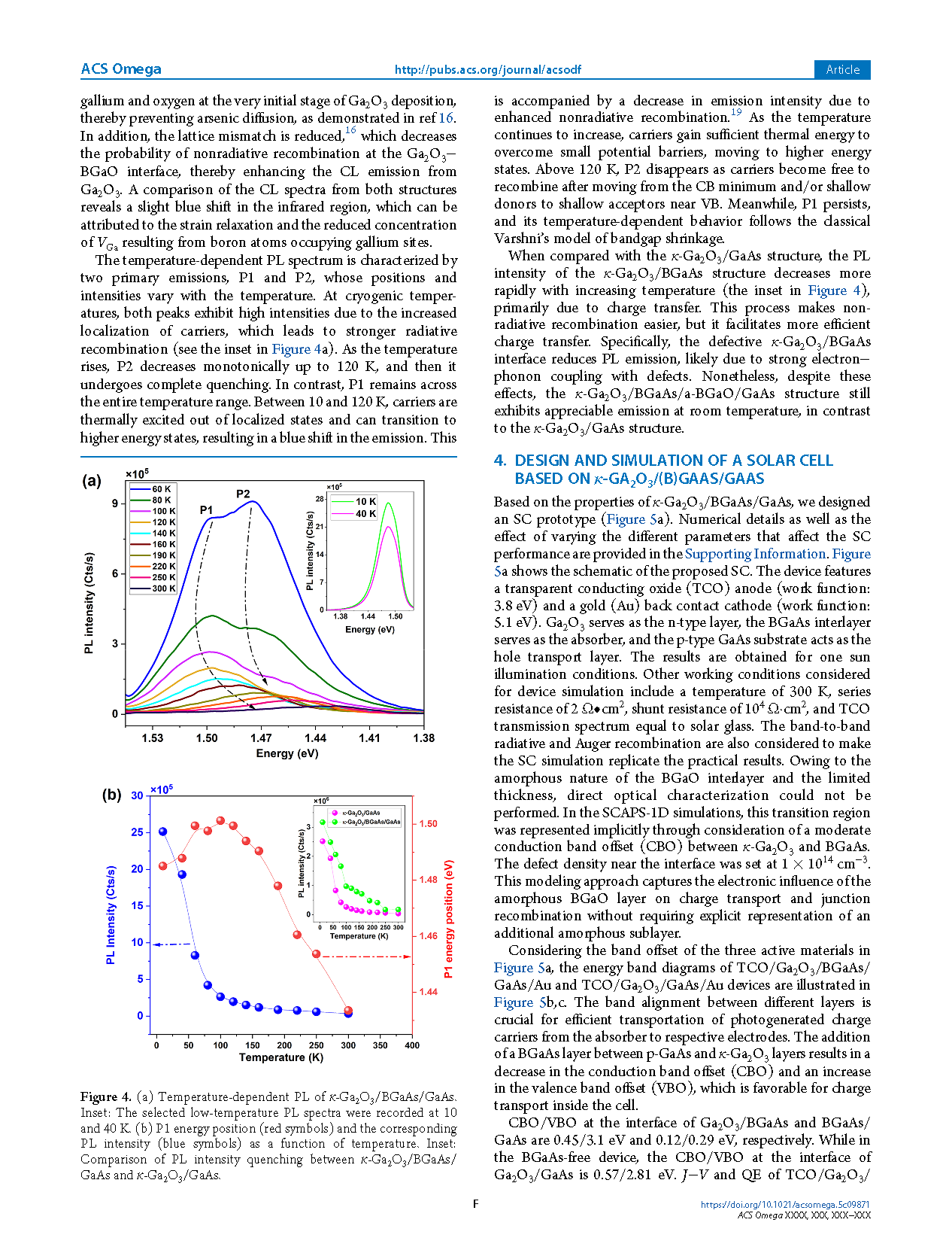
Figure 4. (a) Temperature-dependent PL of κ-Ga2O3/BGaAs/GaAs. Inset: The selected low-temperature PL spectra were recorded at 10 and 40 K. (b) P1 energy position (red symbols) and the corresponding PL intensity (blue symbols) as a function of temperature. Inset: Comparison of PL intensity quenching between κ-Ga2O3/BGaAs/GaAs and κ-Ga2O3/GaAs.
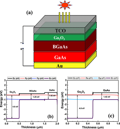
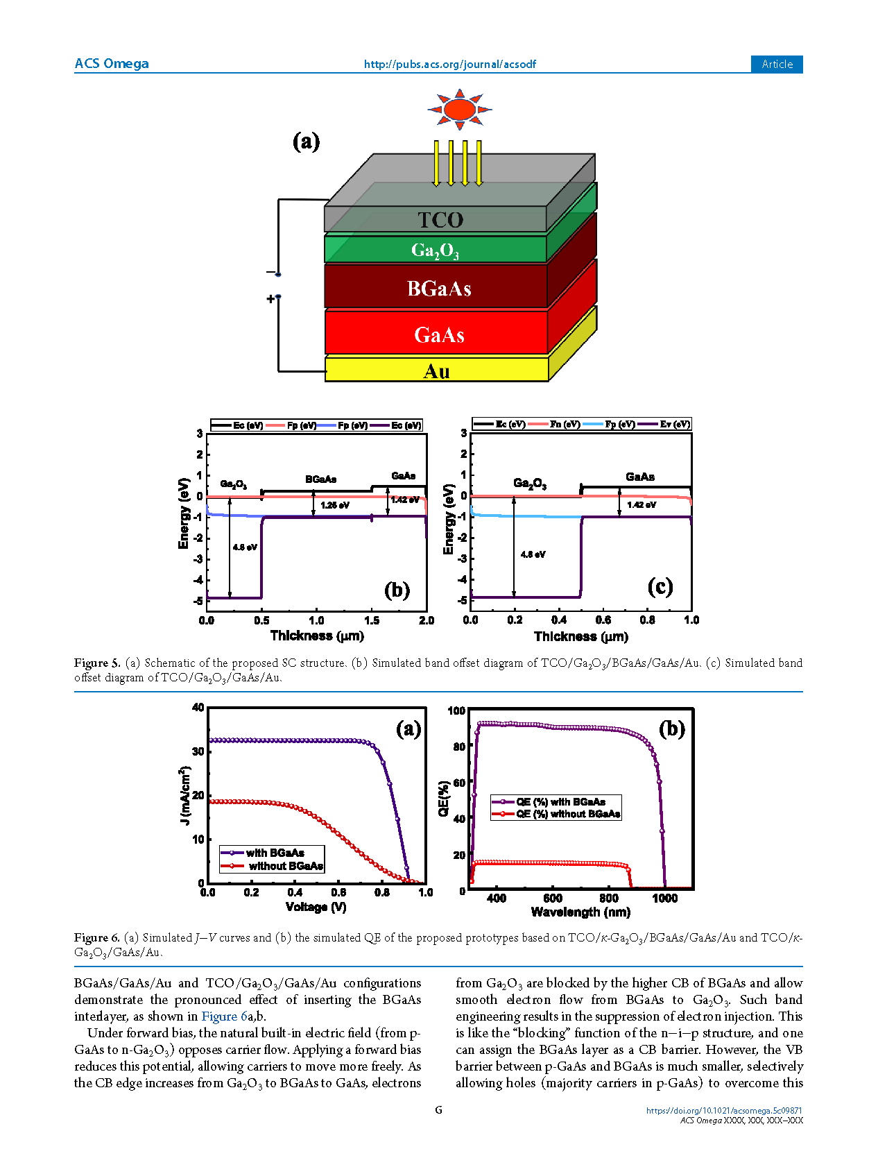
Figure 5. (a) Schematic of the proposed SC structure. (b) Simulated band offset diagram of TCO/Ga2O3/BGaAs/GaAs/Au. (c) Simulated band offset diagram of TCO/Ga2O3/GaAs/Au.
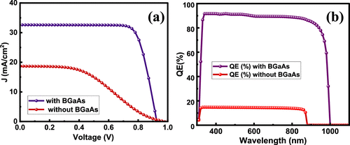
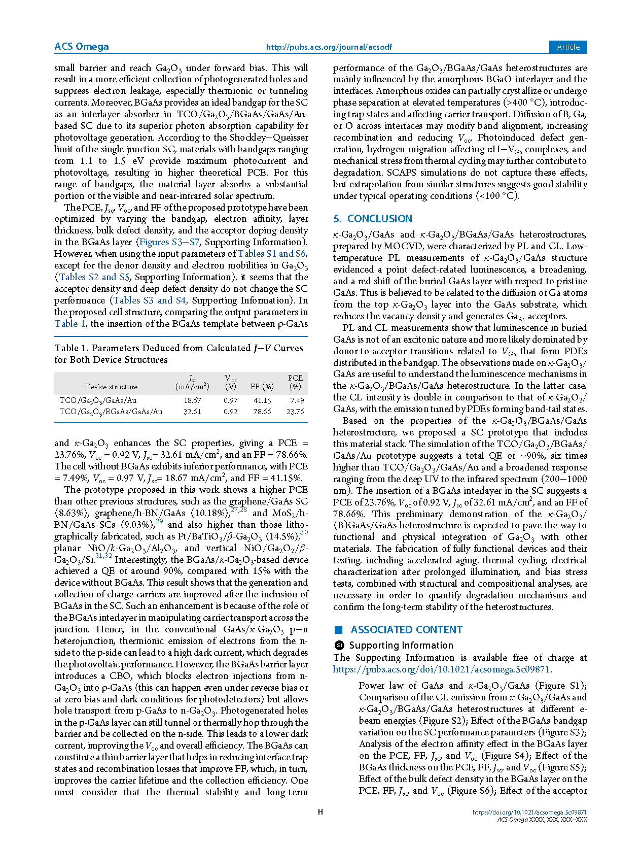
Figure 6. (a) Simulated J–V curves and (b) the simulated QE of the proposed prototypes based on TCO/κ-Ga2O3/BGaAs/GaAs/Au and TCO/κ-Ga2O3/GaAs/Au.
DOI:
doi.org/10.1021/acsomega.5c09871