Paper Sharing
【Member Papers】1200 V / 10 A press-pack gallium oxide Schottky barrier diode under a quasi-uniaxial pressure of more than 20 MPa
日期:2025-12-31阅读:442
Researchers from the Hong Kong University of Science and Technology and Novel Crystal Technology Inc have published a dissertation titled "1200 V / 10 A press-pack gallium oxide Schottky barrier diode under a quasi-uniaxial pressure of more than 20 MPa " in IEEE Electron Device Letters.
Background
Ultra-wide-bandgap semiconductor gallium oxide (β-Ga₂O₃) has a bandgap of approximately 4.8 eV and exhibits tremendous theoretical potential for multi-kilovolt unipolar devices. Its estimated critical breakdown electric field can reach 8 MV/cm, which is 2–3 times that of silicon carbide (SiC) and gallium nitride (GaN). This enables the use of thinner and more heavily doped drift layers, thereby achieving lower on-resistance at the same breakdown voltage. Unlike SiC and GaN, Ga₂O₃ can be grown into large-area, high-quality single-crystal substrates via solution-based methods, significantly reducing the cost of manufacturing high-performance power electronic devices. Owing to these characteristics, β-Ga₂O₃ is regarded as a highly competitive candidate material for power transmission systems, electrified transportation, and pulsed power technologies. In high-voltage power transmission systems, press-pack packaging is widely favored due to its high current-carrying capability, scalable insulation design, excellent mechanical stability, and strong short-circuit robustness. Despite substantial progress in the electrical and thermal properties of β-Ga₂O₃, its mechanical performance remains a major challenge: the material is highly prone to cleavage along the weakly bonded (100) plane. To date, there has been little academic research on whether β-Ga₂O₃ devices can withstand the high pressures required for press-pack packaging.
Abstract
β-Ga2O3 is a competitive candidate for high-voltage power electronics because of its high critical field strength and easy access to high-quality native substrates. Rapid progress has been made in the electrical and thermal performances of β-Ga2O3 devices. However, the mechanical challenges presented by β-Ga2O3 to device packaging have hardly been addressed, specifically in the context of a press-pack package used widely in high-voltage high-capacity power devices. For the first time, this paper validates the feasibility of a β-Ga2O3 press-pack power device utilizing a 1200 V β-Ga2O3 SBD die under a quasi-uniaxial pressure of more than 20 MPa applied to a 200-μm-thick substrate. The reverse leakage current of the press-back β-Ga2O3 SBD remained stable under various pressures ranging from 2 MPa to 20 MPa, which indicated that no mechanical damage or defects that could have degraded the electrical performance were generated. Capacitance–voltage results showed that the Schottky barrier height was unaffected by the quasi-uniaxial pressures in the test range. Higher pressure reduced the contact resistance and the junction-to-case thermal resistance, both of which are beneficial for increasing the power capacity of the press-pack β-Ga2O3 SBD. Under the maximum clamping pressure of 20 MPa, the steady-state junction temperature rise did not exceed 150 K at DC 10 A and a corresponding heating power of over 27 W, from which a junction-to-case thermal resistance of below 5 K/W was determined.
Conclusions
For the first time, this paper validates the feasibility of press-pack packaging for enhancing the power capacity of β-Ga2O3 power devices. Operation of a 1200-V, 200-μm-thick press-pack β-Ga2O3 SBD under a quasi-uniaxial pressure of over 20 MPa without mechanical damage or electrical degradation was demonstrated. The high clamping pressure yielded a low junction-to-case thermal resistance of below 5 K/W at DC 10 A, enabling efficient heat removal from the device that had prevented the junction temperature rise from exceeding 150 K under a heating power of over 27 W. These experimental results have laid the groundwork for the development of press-pack β-Ga2O3 devices toward practical high-power applications.
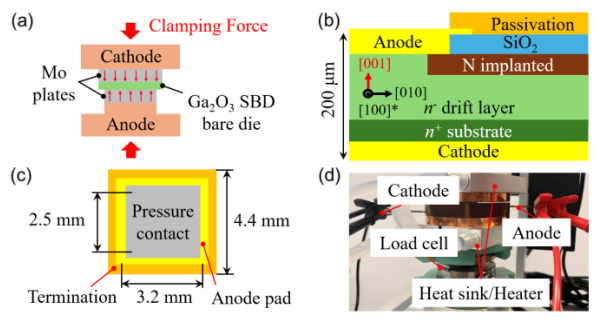
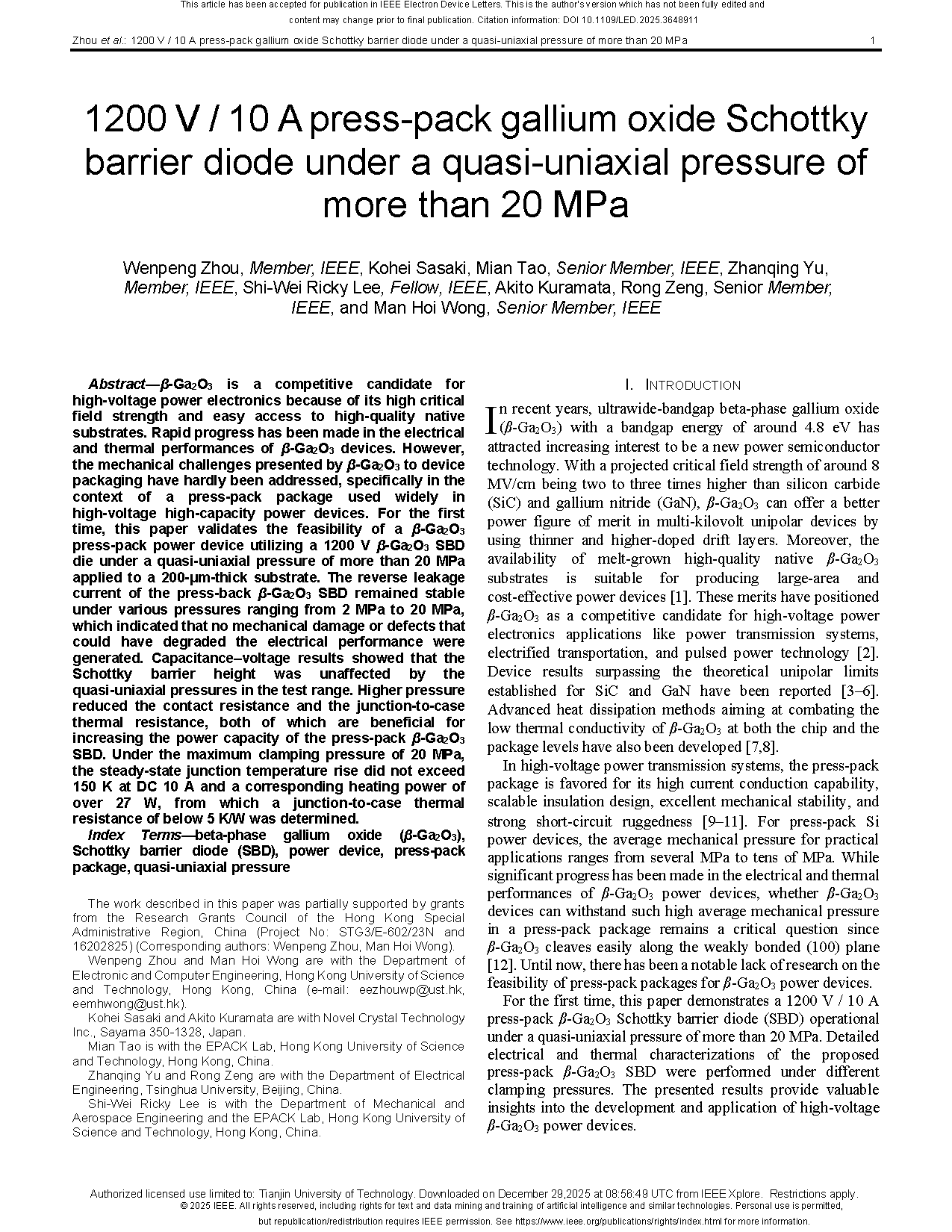
Fig. 1. Illustration of the press-pack β-Ga2O3 SBD and experimental set-up. (a) Design of a press-pack β-Ga2O3 SBD structure. (b) Cross-section of the β-Ga2O3 SBD die. (c) Anode-side view of the β-Ga2O3 SBD die. (d) Photo of the custom-built press-pack experimental setup with double-sided heat sinks or heaters.
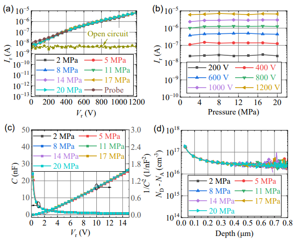
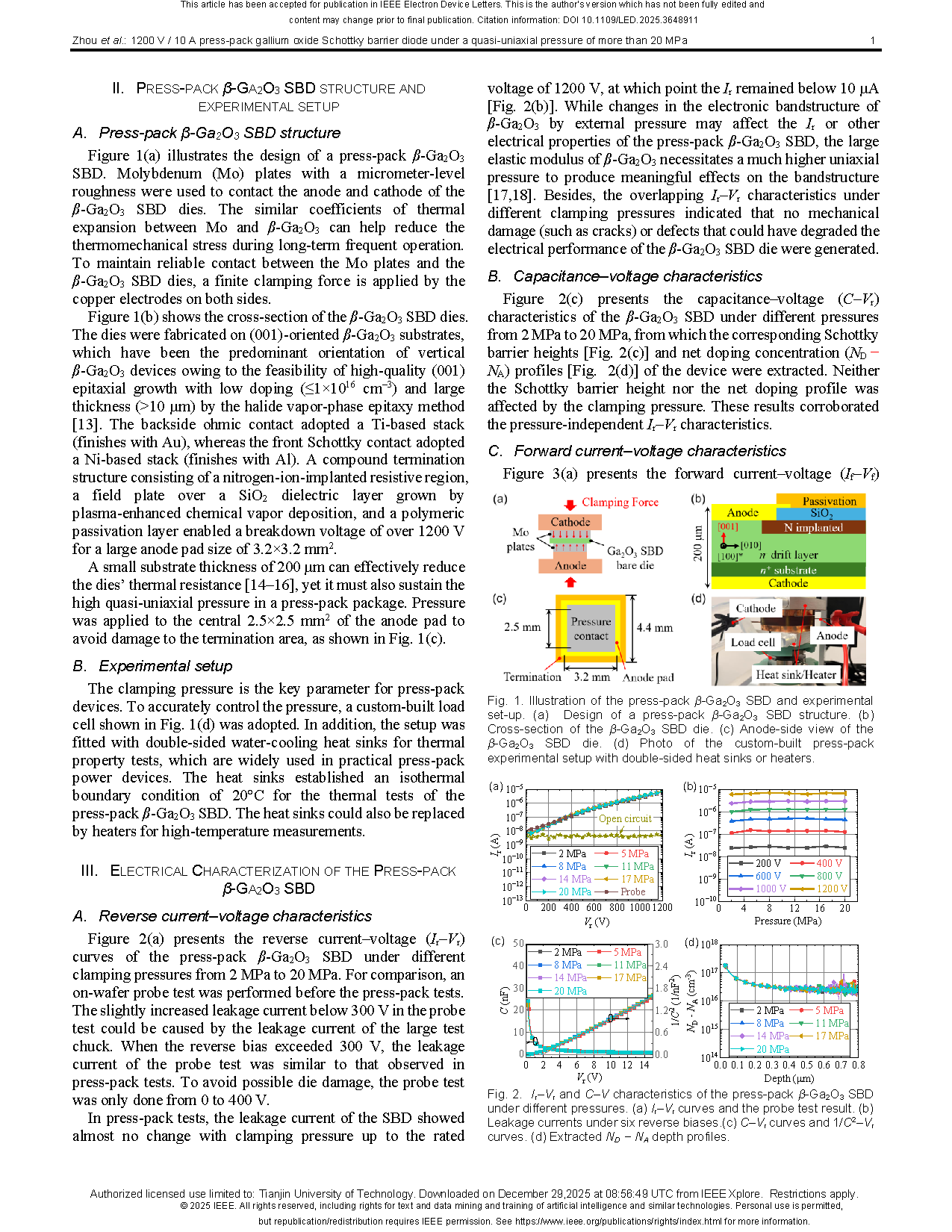
Fig. 2. Ir–Vr and C–V characteristics of the press-pack β-Ga2O3 SBD under different pressures. (a) Ir–Vr curves and the probe test result. (b) Leakage currents under six reverse biases.(c) C–Vr curves and 1/C2–Vr curves. (d) Extracted ND − NA depth profiles.
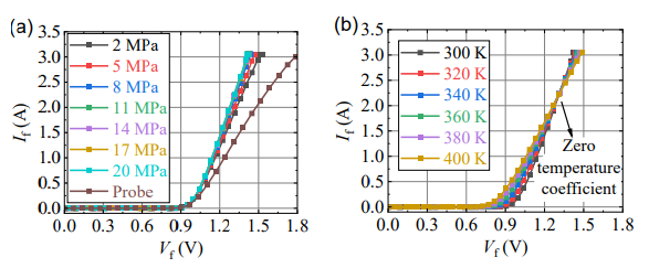
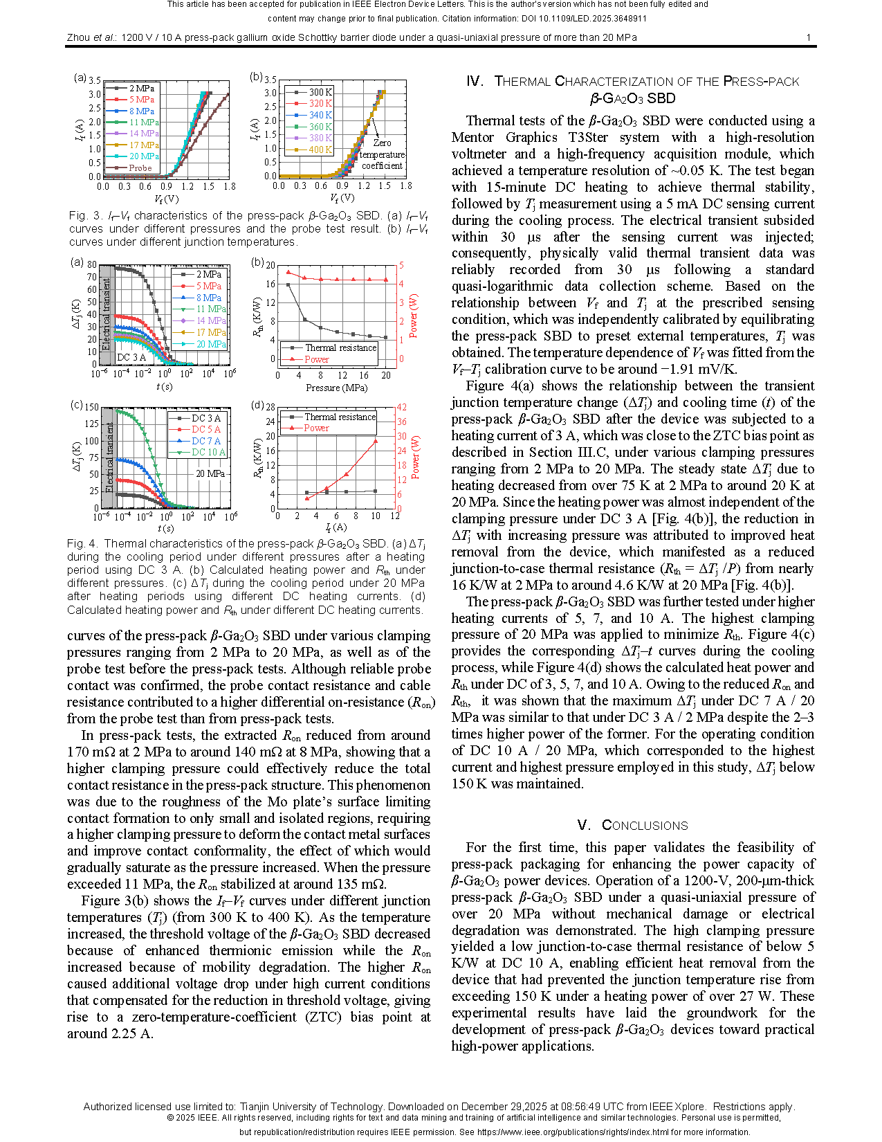
Fig. 3. If–Vf characteristics of the press-pack β-Ga2O3 SBD. (a) If–Vf curves under different pressures and the probe test result. (b) If–Vf curves under different junction temperatures.
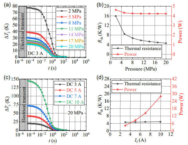
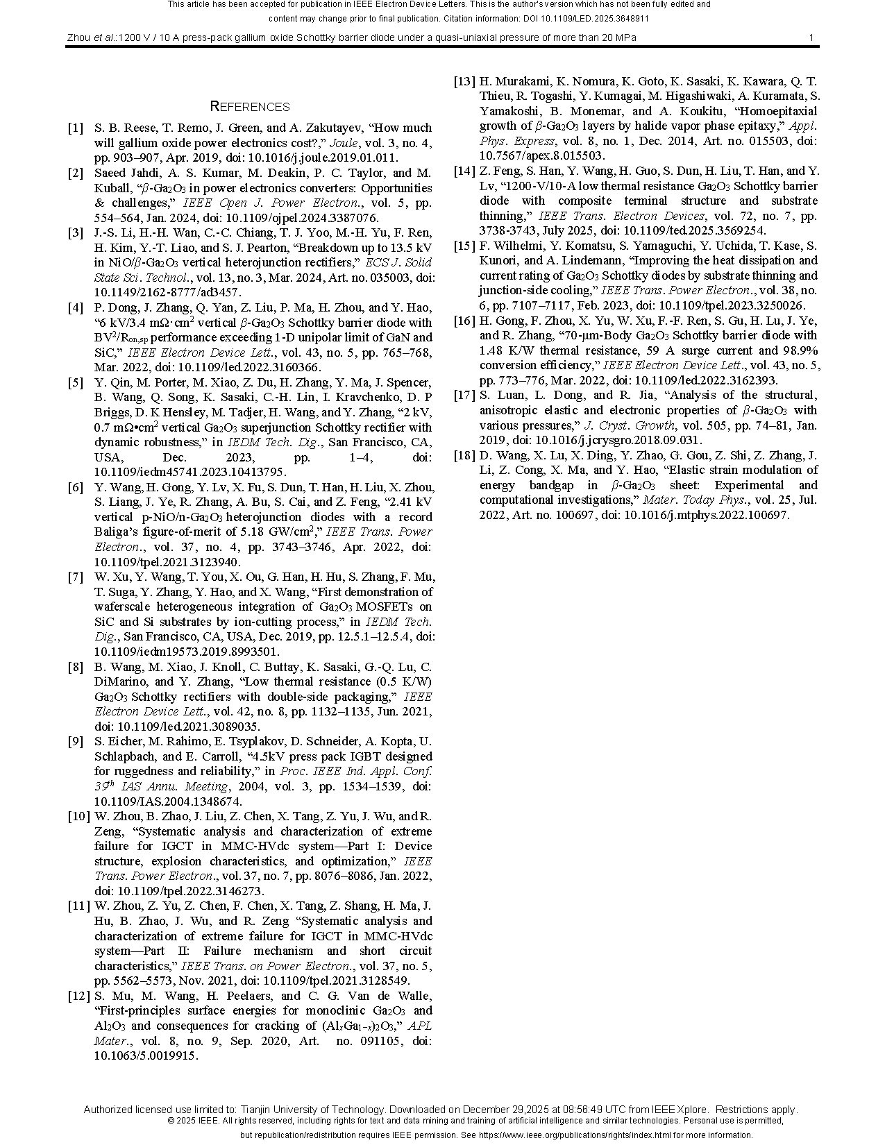
Fig. 4. Thermal characteristics of the press-pack β-Ga2O3 SBD. (a) ΔTj during the cooling period under different pressures after a heating period using DC 3 A. (b) Calculated heating power and Rth under different pressures. (c) ΔTj during the cooling period under 20 MPa after heating periods using different DC heating currents. (d) Calculated heating power and Rth under different DC heating currents.
DOI:
doi.org/10.1109/LED.2025.3648911