Paper Sharing
【Domestic Papers】Defect-Mediated Threshold Voltage Tuning in β-Ga₂O₃ MOSFETs via Fluorine Plasma Treatment
日期:2026-01-04阅读:441
Researchers from the Sun Yat-Sen University have published a dissertation titled "Defect-Mediated Threshold Voltage Tuning in β-Ga2O3 MOSFETs via Fluorine Plasma Treatment" in Nanomaterials.
Project Support
This research was funded by the National Natural Science Foundation of China (No. U22A2073, 62474197). Guangdong Basic and Applied Basic Research Foundation (2024A1515011536). Guangzhou Basic and Applied Basic Research Foundation (2025A04J7142).
Background
With the continuous advancement of power-device scaling driven by demands for high power density and miniaturization, silicon (Si)-based power devices are confronting fundamental physical limitations. The relatively low critical electric field of Si (≤0.3 MV/cm) restricts further reduction in device dimensions while maintaining breakdown robustness, motivating the development of wide-bandgap semiconductor technologies. Materials such as GaN, SiC, and Ga2O3 offer distinct advantages in this regard. These materials exhibit superior Baliga’s figure of merit (BFOM), enabling the development of smaller, faster, more efficient, and reliable electronic devices.
In this work, we apply fluorine plasma surface engineering to plasma-assisted molecular beam epitaxy (PA-MBE) grown β-Ga2O3 films on 2-inch sapphire substrates and demonstrate its simultaneous impact on threshold voltage tuning and breakdown enhancement in lateral MOSFETs. The F treatment effectively reduces near-surface donor-like states, enabling an ultralow Ioff of 1 × 10⁻⁹ mA/mm and a controllable positive Vth shift up to +12.4 V by adjusting the plasma duration. XPS analysis reveals F incorporation and the formation of F–Ga-related bonding, while TCAD simulations suggest that the suppressed near-surface charge and the widened depletion region are responsible for the experimentally observed increase in breakdown voltage. These results clarify the role of fluorine in modifying surface defect states in PA-MBE β-Ga2O3 and provide an effective route for engineering threshold voltage and leakage in Ga2O3-based power devices.
Abstract
We demonstrate high-performance MOSFETs on β-Ga2O3 films grown by plasma-assisted molecular beam epitaxy (PA-MBE). The high crystalline quality of the β-Ga2O3 epilayer was confirmed by X-ray diffraction and atomic force microscopy. An optimized CF4-plasma treatment was employed to introduce fluorine (F) into the near-surface region, effectively suppressing donor-like states. The resulting devices exhibit an ultralow off-state current of 1 × 10⁻⁹ mA/mm and a stable on/off ratio of 105. A controllable positive threshold voltage shift up to +12.4 V was achieved by adjusting the plasma duration. X-ray photoelectron spectroscopy indicates that incorporated F atoms form F–Ga-related bonds and compensate oxygen-related donor defects. Sentaurus TCAD simulations reveal reduced near-surface charge and a widened depletion region, providing a physical explanation for the experimentally observed increase in breakdown voltage from 453 V to 859 V. These results clarify the role of fluorine in modulating surface defect states in PA-MBE β-Ga2O3 and demonstrate an effective route for threshold-voltage engineering and leakage suppression in Ga2O3 power devices.
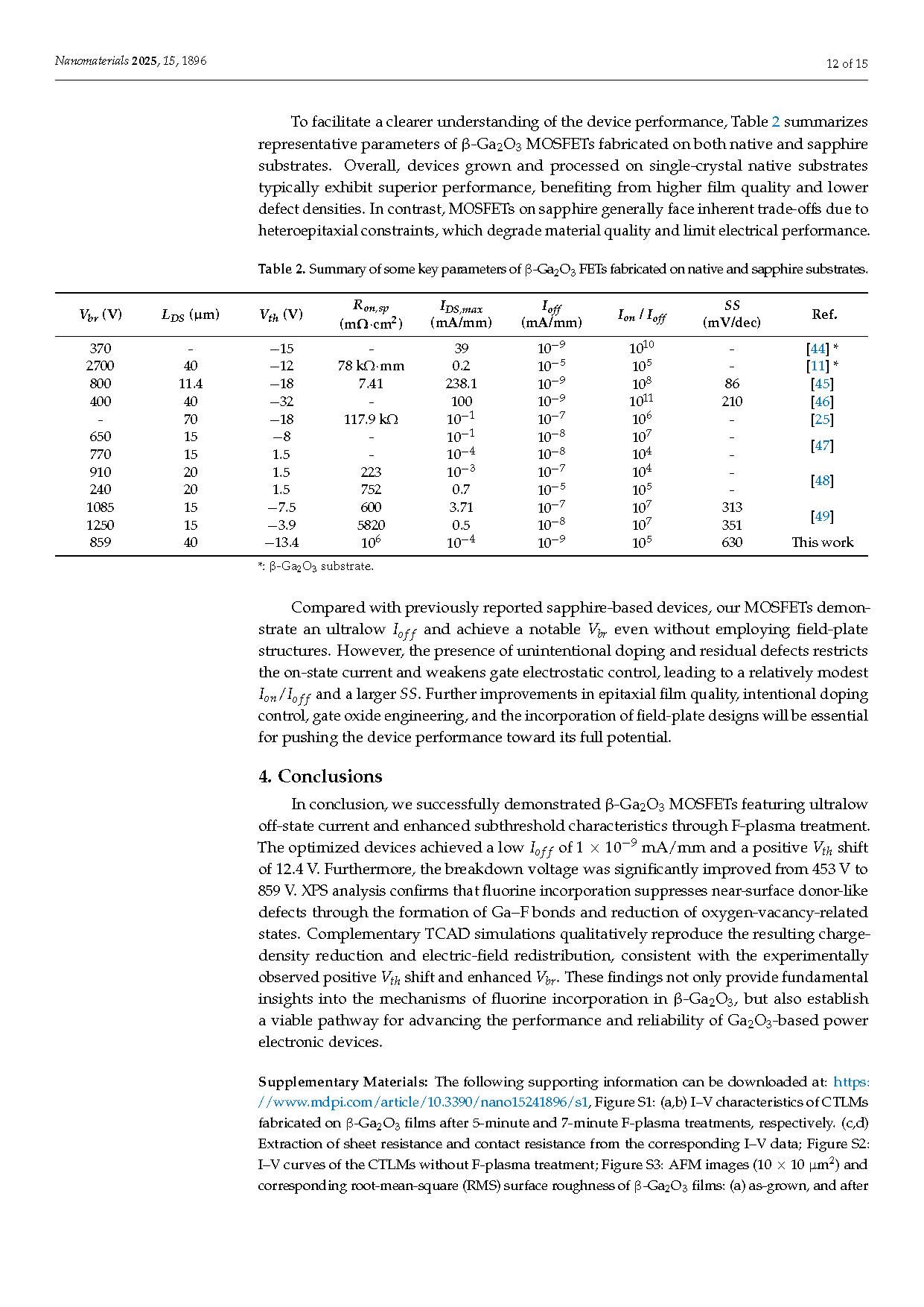
Conclusions
In conclusion, we successfully demonstrated β-Ga2O3 MOSFETs featuring ultralow off-state current and enhanced subthreshold characteristics through F-plasma treatment. The optimized devices achieved a low Ioff of 1 × 10⁻⁹ mA/mm and a positive Vth shift of 12.4 V. Furthermore, the breakdown voltage was significantly improved from 453 V to 859 V. XPS analysis confirms that fluorine incorporation suppresses near-surface donor-like defects through the formation of Ga–F bonds and reduction of oxygen-vacancy-related states. Complementary TCAD simulations qualitatively reproduce the resulting charge-density reduction and electric-field redistribution, consistent with the experimentally observed positive Vth shift and enhanced Vbr. These findings not only provide fundamental insights into the mechanisms of fluorine incorporation in β-Ga2O3, but also establish a viable pathway for advancing the performance and reliability of Ga2O3-based power electronic devices.
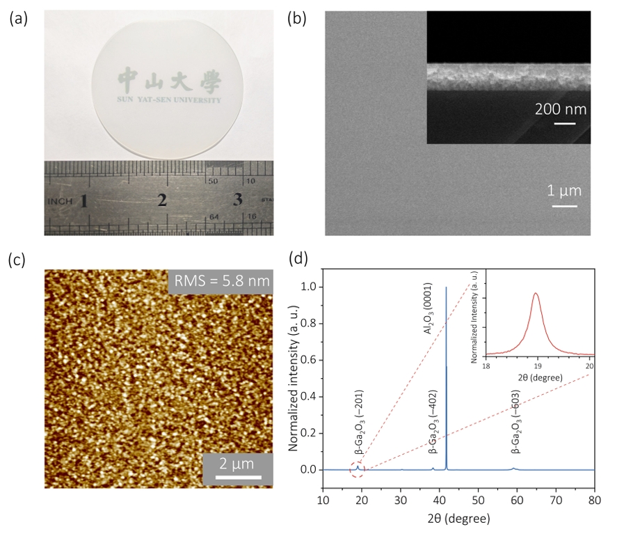
Figure 1. Optical image and crystalline properties of the β-Ga2O3 film grown on a 2-inch sapphire substrate via plasma-assisted molecular beam epitaxy (PA-MBE). (a) Optical image of the as-grown 2-inch β-Ga2O3 thin film wafer. (b) Scanning electron microscopy (SEM) image of the single-crystalline β-Ga2O3 film obtained by heteroepitaxy. Inset: cross-sectional SEM image showing a film thickness of approximately 300 nm. (c) Atomic force microscopy (AFM) image of the film surface with a root-mean-square (RMS) roughness of 5.8 nm. (d) X-ray diffraction (XRD) pattern of the β-Ga2O3 film on sapphire substrate. The three characteristic peaks located at 18.9°, 38.4° and 59.0° are related to the (−201), (−402) and (−603) lattice planes of β-Ga2O3, respectively. Inset: enlarged view of the (−201) peak, with a full width at half maximum (FWHM) of 0.31°, confirming the high crystallinity of the β-Ga2O3 film.
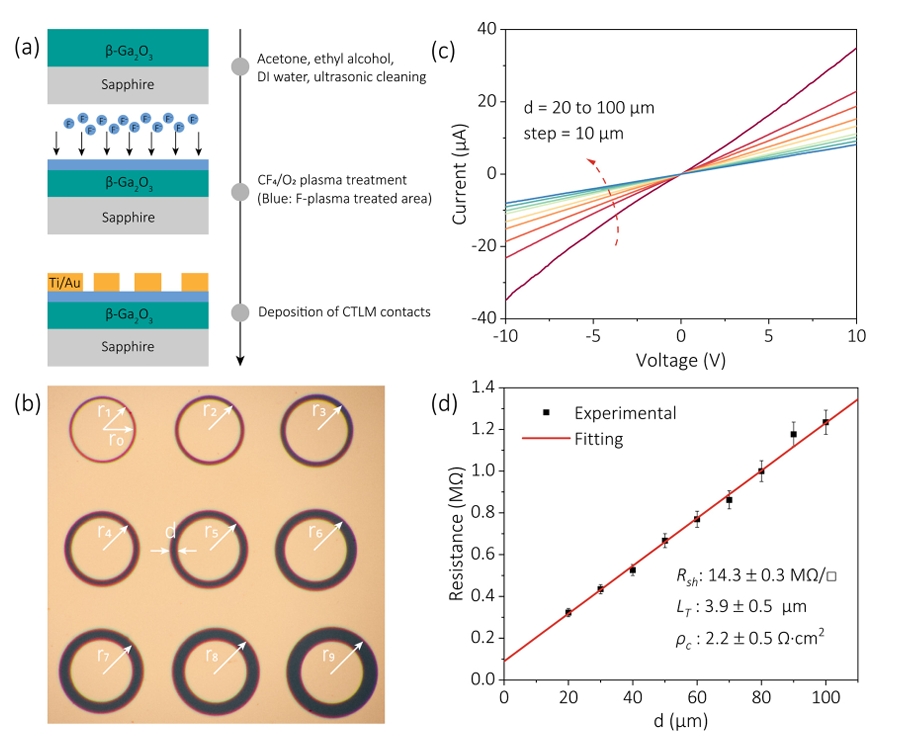
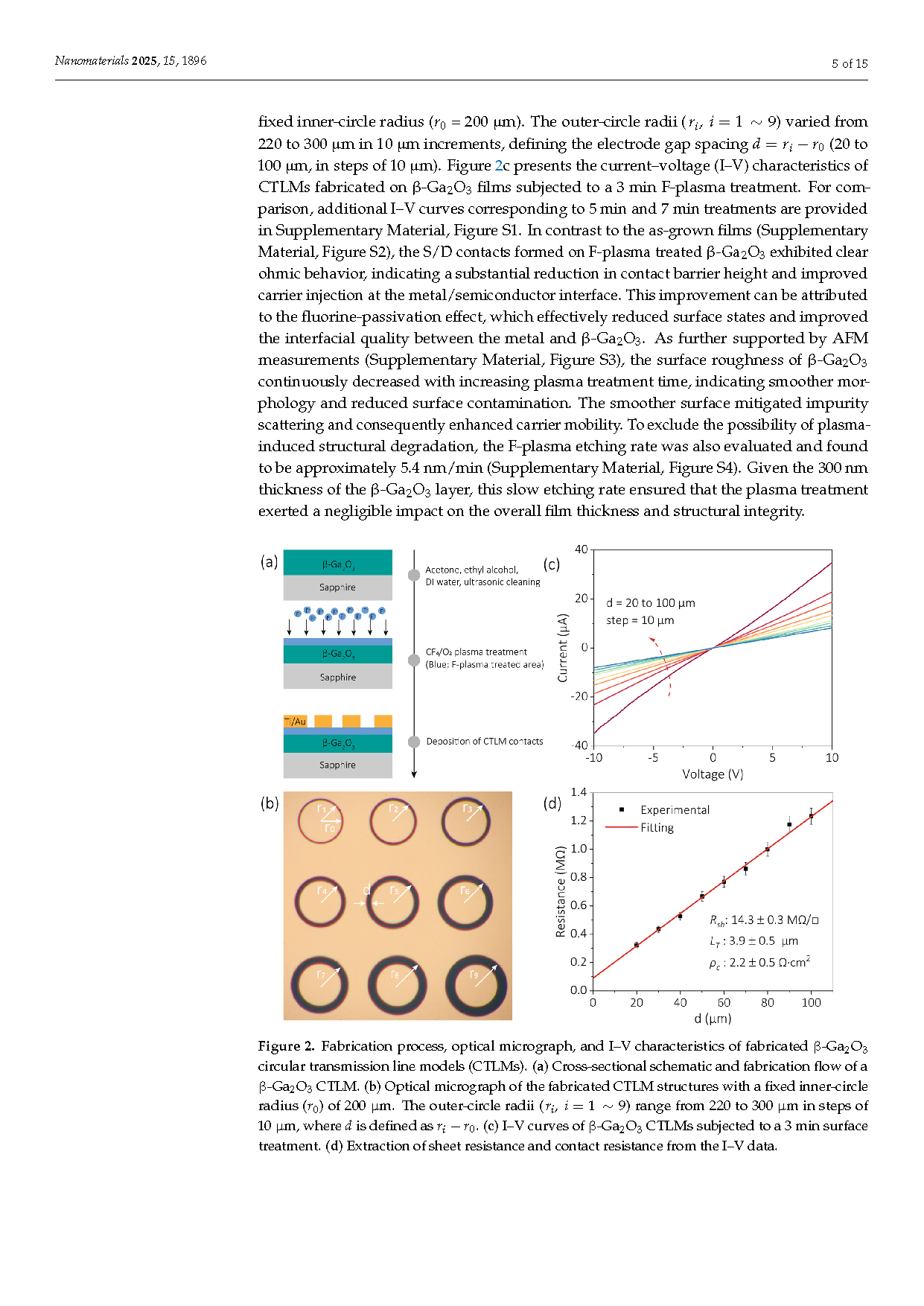
Figure 2. Fabrication process, optical micrograph, and I–V characteristics of fabricated β-Ga2O3 circular transmission line models (CTLMs). (a) Cross-sectional schematic and fabrication flow of a β-Ga2O3 CTLM. (b) Optical micrograph of the fabricated CTLM structures with a fixed inner-circle radius (r0) of 200 μm. The outer-circle radii (ri, i=1~9) range from 220 to 300 μm in steps of 10 μm, where d is defined as ri−r0. (c) I–V curves of β-Ga2O3 CTLMs subjected to a 3 min surface treatment. (d) Extraction of sheet resistance and contact resistance from the I–V data.

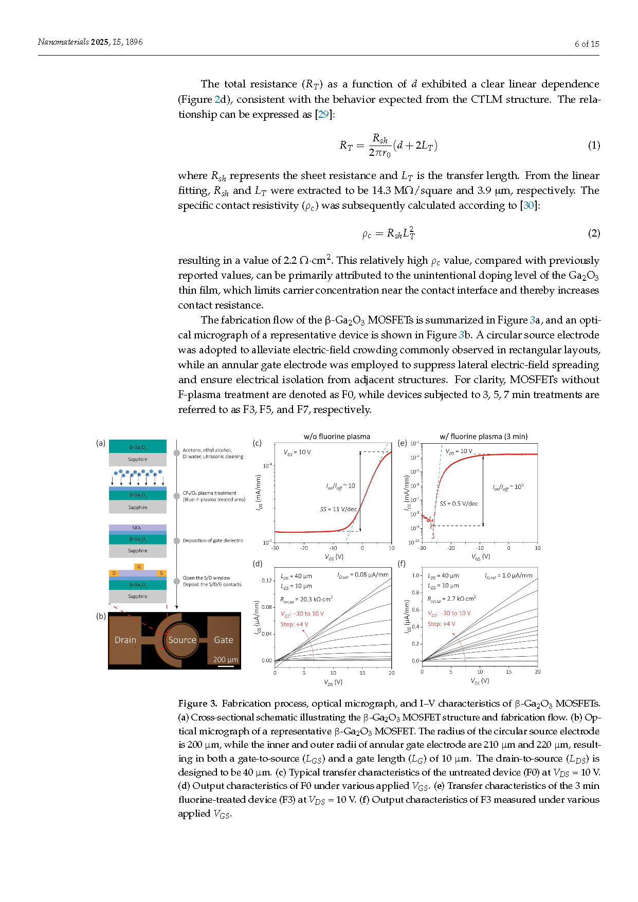
Figure 3. Fabrication process, optical micrograph, and I–V characteristics of β-Ga2O3 MOSFETs. (a) Cross-sectional schematic illustrating the β-Ga2O3 MOSFET structure and fabrication flow. (b) Optical micrograph of a representative β-Ga2O3 MOSFET. The radius of the circular source electrode is 200 μm, while the inner and outer radii of annular gate electrode are 210 μm and 220 μm, resulting in both a gate-to-source (LGS) and a gate length (LG) of 10 μm. The drain-to-source (LDS) is designed to be 40 μm. (c) Typical transfer characteristics of the untreated device (F0) at VDS = 10 V. (d) Output characteristics of F0 under various applied VGS. (e) Transfer characteristics of the 3 min fluorine-treated device (F3) at VDS = 10 V. (f) Output characteristics of F3 measured under various applied VGS.

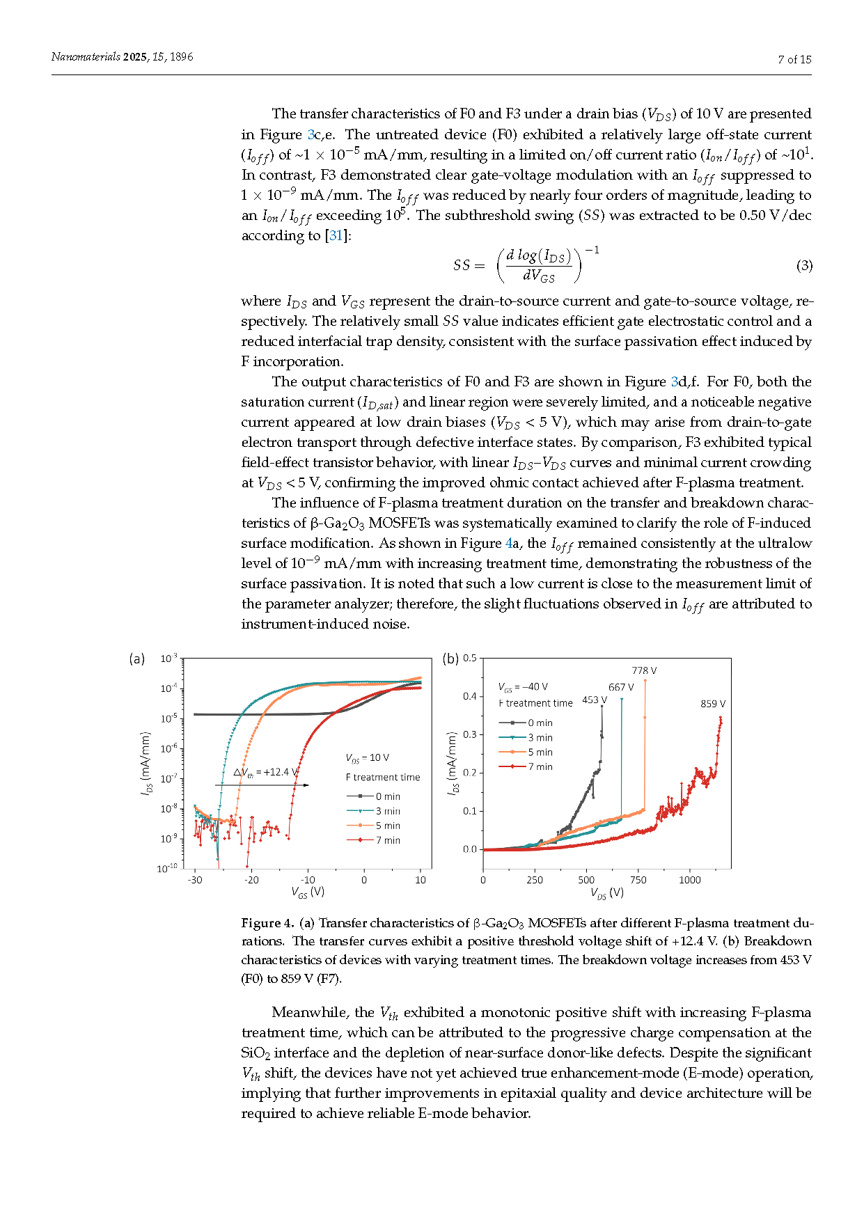
Figure 4. (a) Transfer characteristics of β-Ga2O3 MOSFETs after different F-plasma treatment durations. The transfer curves exhibit a positive threshold voltage shift of +12.4 V. (b) Breakdown characteristics of devices with varying treatment times. The breakdown voltage increases from 453 V (F0) to 859 V (F7).
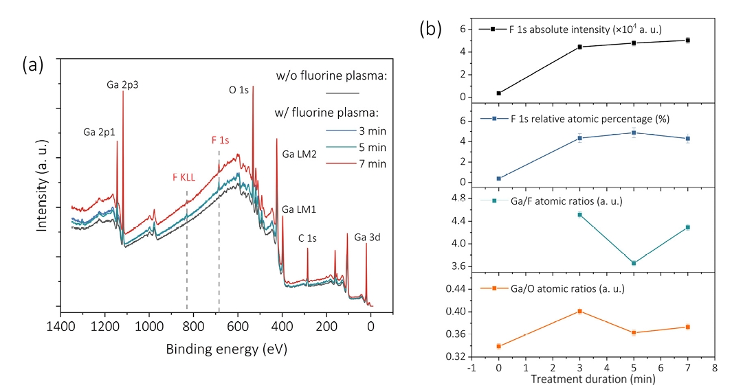
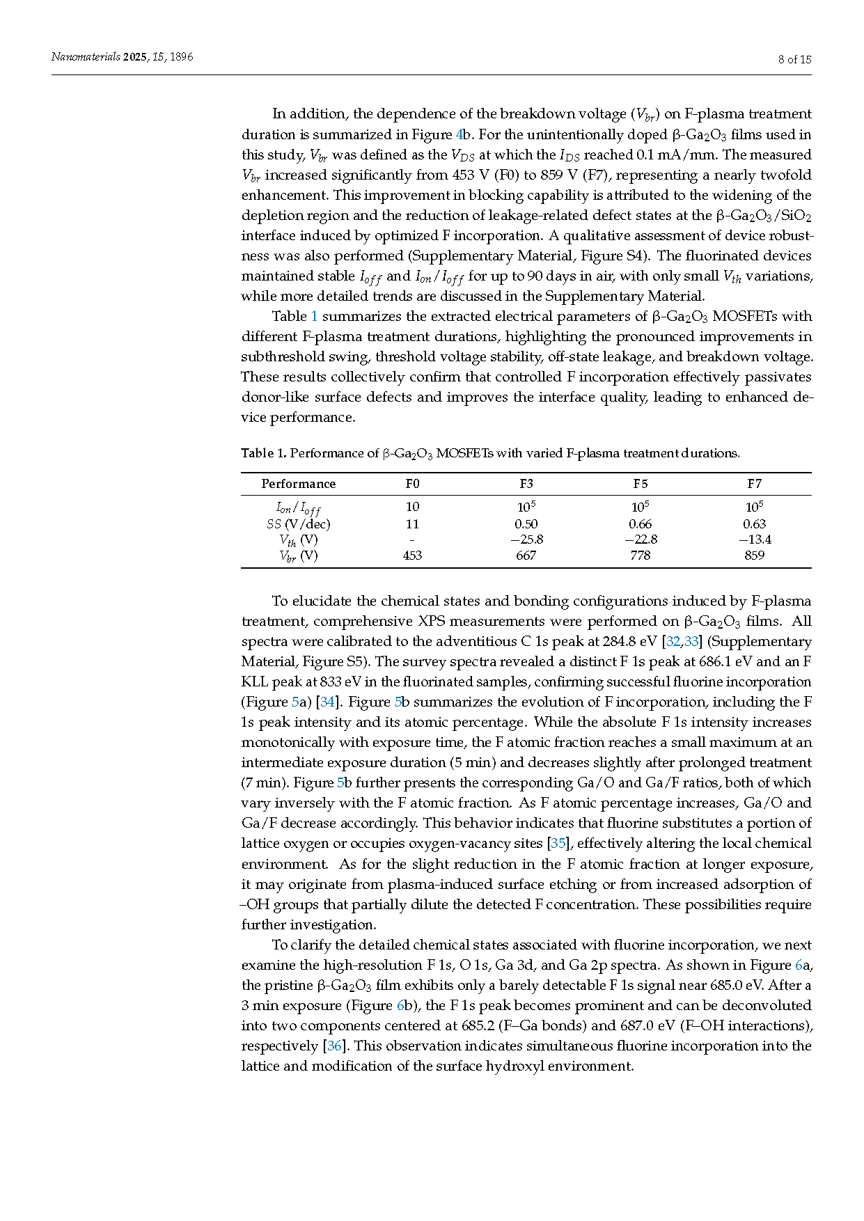
Figure 5. (a) X-ray photoelectron spectroscopy (XPS) survey spectra of the pristine and fluorinated β-Ga2O3 surfaces, revealing the emergence of the F 1s and F KLL peaks after F-plasma treatment. (b) Time-dependent evolution of the absolute F 1s intensity, the relative F 1s atomic percentage, and the Ga/F and Ga/O atomic ratios for samples subjected to F-plasma treatment.
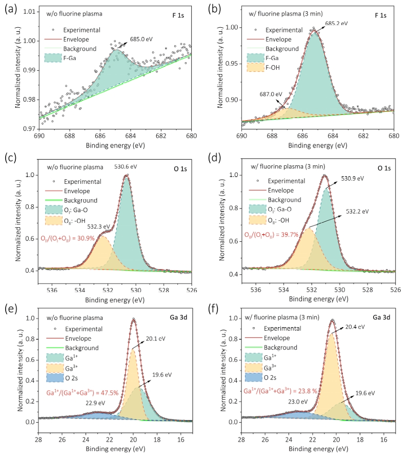
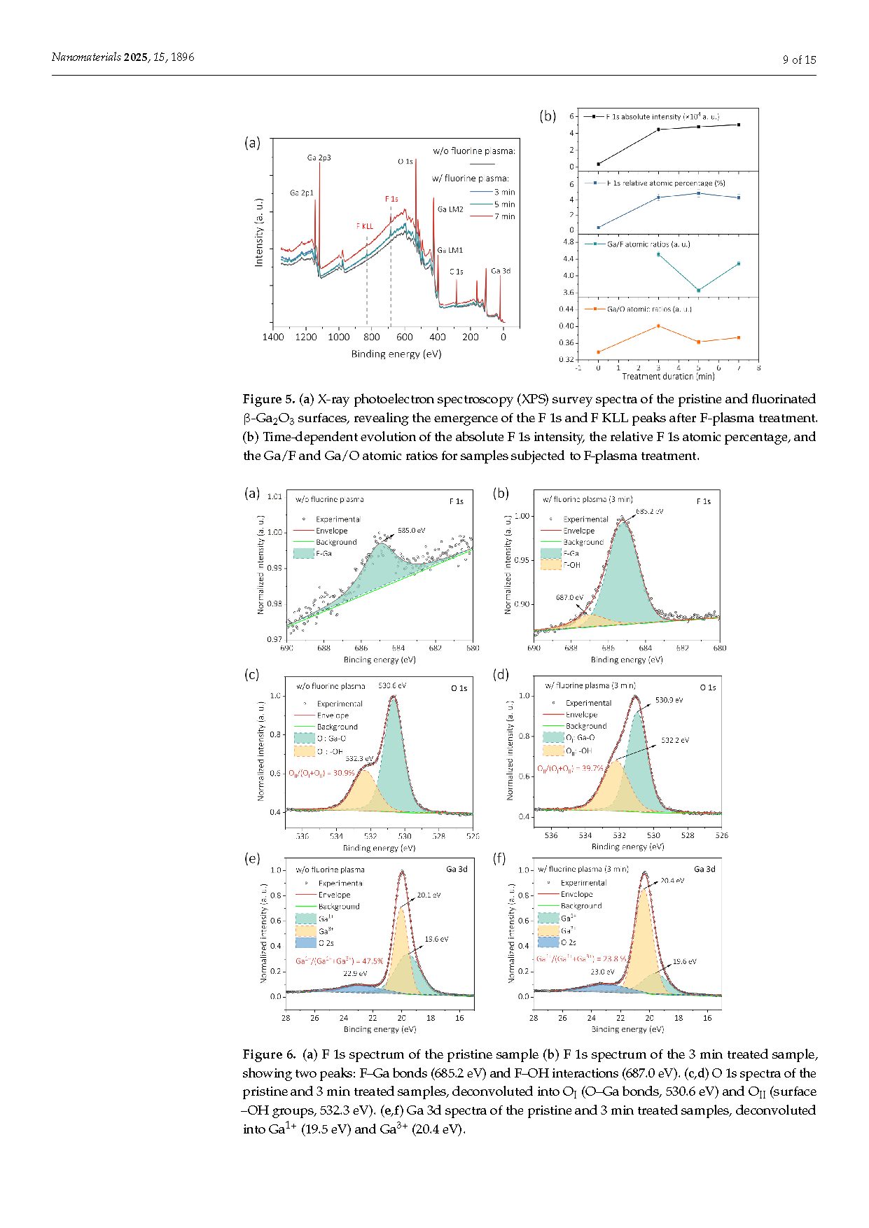
Figure 6. (a) F 1s spectrum of the pristine sample (b) F 1s spectrum of the 3 min treated sample, showing two peaks: F–Ga bonds (685.2 eV) and F–OH interactions (687.0 eV). (c,d) O 1s spectra of the pristine and 3 min treated samples, deconvoluted into OI (O–Ga bonds, 530.6 eV) and OII (surface –OH groups, 532.3 eV). (e,f) Ga 3d spectra of the pristine and 3 min treated samples, deconvoluted into Ga1+ (19.5 eV) and Ga3+ (20.4 eV).
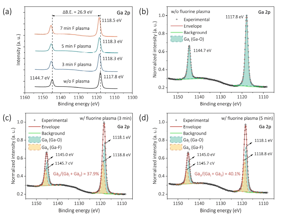
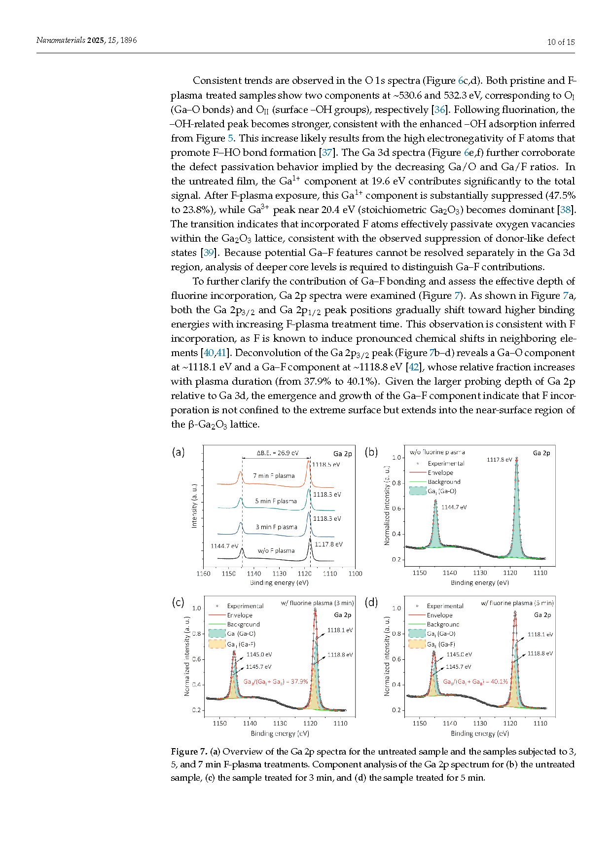
Figure 7. (a) Overview of the Ga 2p spectra for the untreated sample and the samples subjected to 3, 5, and 7 min F-plasma treatments. Component analysis of the Ga 2p spectrum for (b) the untreated sample, (c) the sample treated for 3 min, and (d) the sample treated for 5 min.
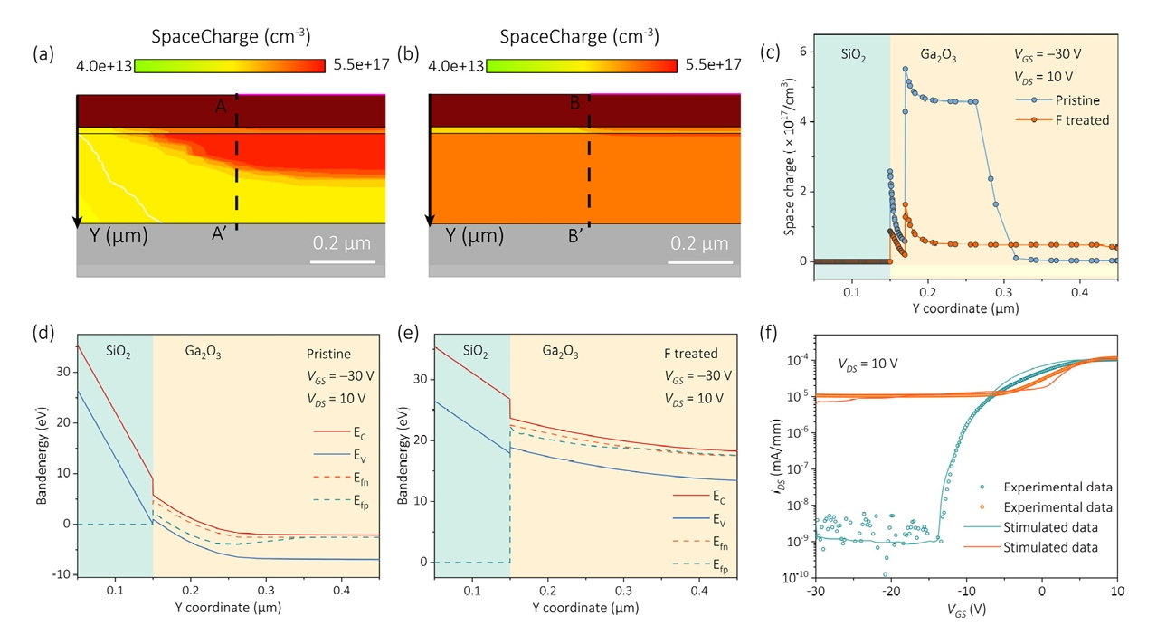
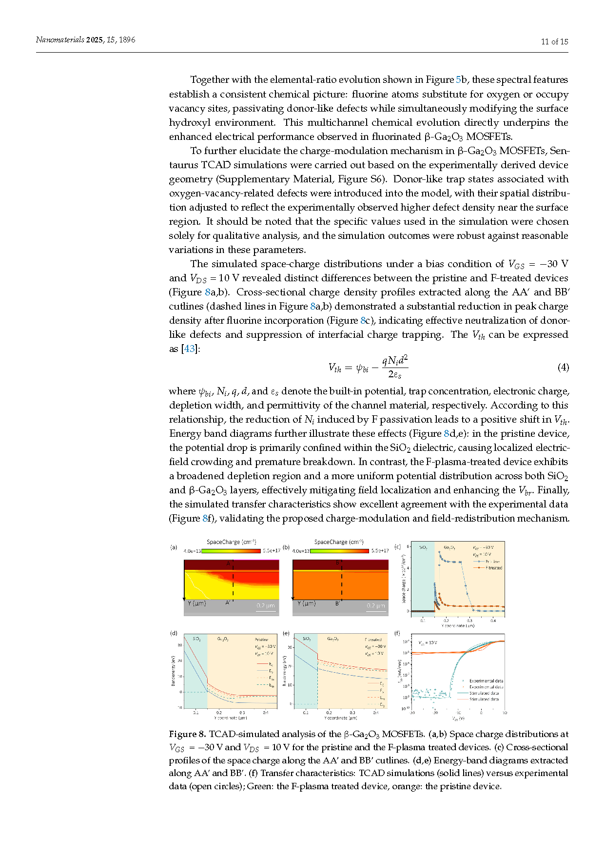
Figure 8. TCAD-simulated analysis of the β-Ga2O3 MOSFETs. (a,b) Space charge distributions at VGS = −30 V and VDS = 10 V for the pristine and the F-plasma treated devices. (c) Cross-sectional profiles of the space charge along the AA’ and BB’ cutlines. (d,e) Energy-band diagrams extracted along AA’ and BB’. (f) Transfer characteristics: TCAD simulations (solid lines) versus experimental data (open circles); Green: the F-plasma treated device, orange: the pristine device.
DOI:
doi.org/10.3390/nano15241896