Paper Sharing
【International Papers】Characterization of strain effects on structure, surface morphology, and band gap of MOVPE grown β-Ga₂O₃ thin films on β-(AlₓGa₁₋ₓ)₂O₃ substrates
日期:2026-01-15阅读:361
Researchers from the Leibniz-Institut für Kristallzüchtung (IKZ) have published a dissertation titled "Characterization of strain effects on structure, surface morphology, and band gap of MOVPE grown β-Ga2O3 thin films on β-(AlxGa1−x)2O3 substrates" in Journal of Physics D: Applied Physics.
Background
Beta-gallium oxide (β-Ga2O3) is a semiconductor material that has attracted considerable attention for next-generation power electronics, particularly due to its ultra-wide bandgap of approximately 4.9 eV and a theoretical electric field breakdown strength as high as 8 MV cm−1. The monoclinic β-phase of (AlxGa1−x)2O₃ has also gained significant interest due to bandgap enlargement and potential applications in the ultraviolet spectral region. The epitaxial growth of β-(AlxGa1−x)2O₃ on β-Ga2O3 substrates has been investigated using molecular beam epitaxy and metal-organic vapor phase epitaxy (MOVPE). However, recent studies by Galazka et al have shown that the room-temperature electron mobility in β-(AlxGa1−x)2O₃ decreases with increasing aluminum content at comparable free electron concentrations. The epitaxial growth of β-Ga2O3 films on β-(AlxGa1−x)2O₃ substrates is representing an interesting alternative but has not yet been investigated due to the lack of suitable substrates.
Lattice mismatch plays a critical role in heteroepitaxy. When semiconductor materials with minimal lattice mismatch are epitaxially grown, the thin film adapts the in-plane lattice parameters of the underlying substrate. Owing to the Poisson effect, this results in a vertical strain in the epitaxial layer. It is widely recognized that the bandgap of the grown films is influenced by the lattice modifications induced by epitaxial growth on mismatched substrates. The band gap of the strained layer increases under compression and decreases under tension.
Abstract
β-Ga2O3 thin films (∼83 nm) were grown on β-(AlxGa1−x)2O₃ (x = 0.1, 0.15, 0.2) (100) substrates via metal-organic vapor phase epitaxy (MOVPE) and characterized by high resolution x-ray diffraction (HR-XRD), atomic force microscopy (AFM) and spectroscopic ellipsometry (SE). HR-XRD confirmed the coherent epitaxial growth of β-Ga2O3 thin films, with the strain state exhibiting a direct dependence on the aluminum composition (x) in the substrate. AFM showed a surface roughness of about 0.3 nm which is not affected by the incorporated epitaxial strain. Thickness dependence of β-Ga2O3 grown on β-(AlxGa1−x)2O₃ (x = 0.2) was investigated, revealing that the film remained fully strained up to a thickness of 247 nm and maintained smooth surfaces. Band gap energies for films (83 nm) grown under compressive lattice strain were determined by SE in a large energy range between 1.5–6.5 eV using the Tauc–Lorentz dispersion model. While the band gap of the substrate increases linearly with increasing Al content, a slight enhancement in the band gap of the film was observed with increasing Al content up to x = 0.15, beyond which no further change was detected at x= 0.2. These results suggest that the MOVPE technique is promising for producing β-Ga2O3 with controlled band gap and developing heterojunction devices.
Conclusion
In summary, we demonstrated MOVPE heteroepitaxial growth of β-Ga2O3 thin films (83 nm) on (100) β-(AlxGa1−x)2O₃ (x = 0.1, 0.15, 0.2) substrates. The results demonstrate that the films are coherently grown and the incorporated strain increases linearly with the Al content (x) in the substrate. The grown films exhibit smooth surfaces with rms roughness of about 0.3 nm, independent of the epitaxial strain. A thicker β-Ga2O3 film, up to 247 nm was coherently grown on a β-(AlxGa1−x)2O₃ substrate with x = 0.2, exhibiting a smooth surface morphology. While the band gap of the β-(AlxGa1−x)2O₃ substrate linearly increases with the Al content (x), the band gap of the β-Ga2O3 films initially exhibits a slight increase and then remains approximately constant as x continues to increase. The slight increase in the band gap of the β-Ga2O3 films compared to that of the β-(AlxGa1−x)2O₃ substrates is advantageous to maintain the band gap difference for heterojunctions in electronic devices.
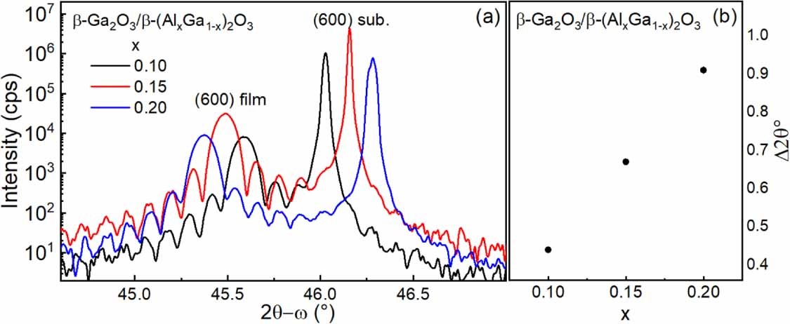
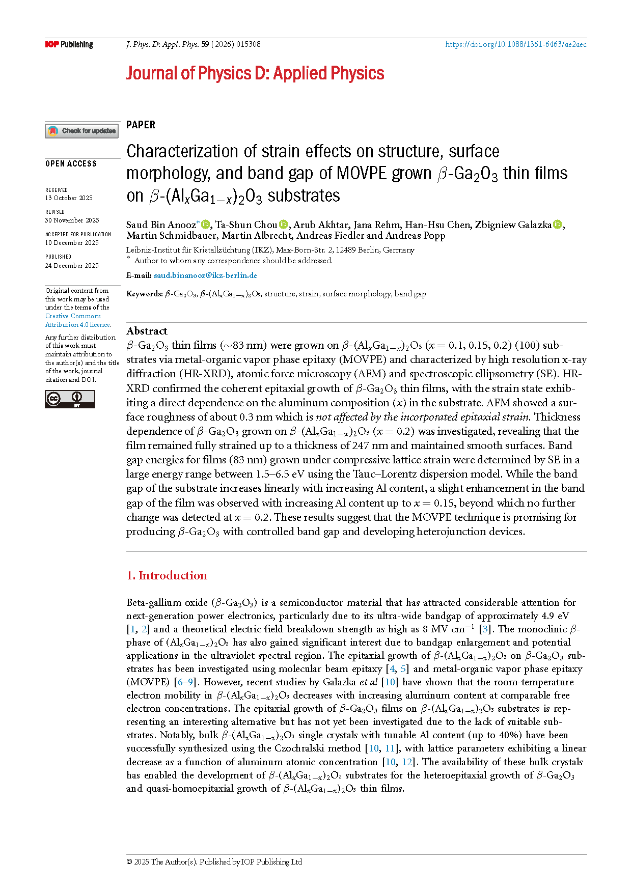
Figure 1. (a) HR-XRD 2θ–ω scans of β-Ga2O3 thin films grown on β-(AlxGa1−x)2O₃ (x = 0.1, 0.15 and 0.2) substrates. (b) Experimental peak spacing (Δ2θ) between substrate and film Bragg reflections as a function of the Aluminum content x.
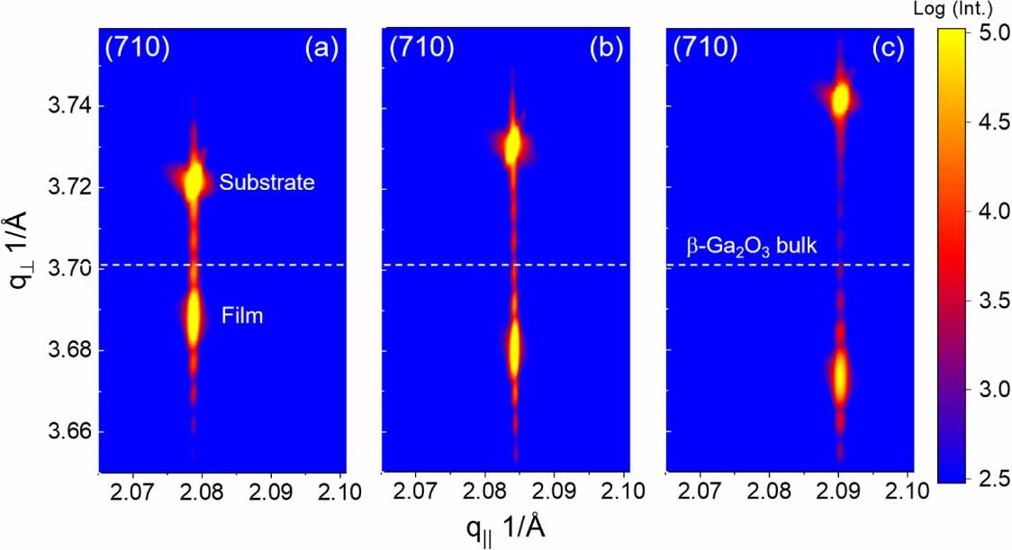
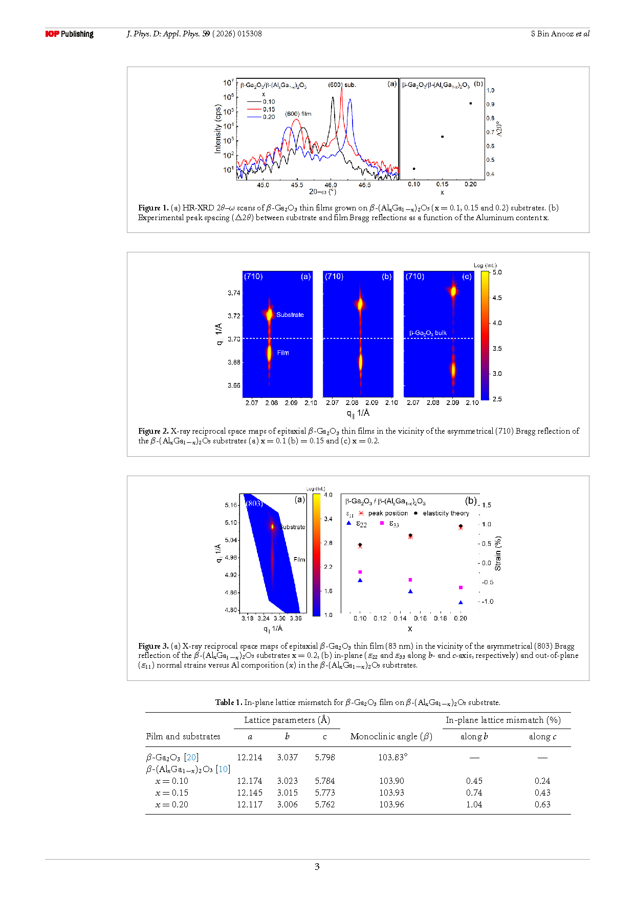
Figure 2. X-ray reciprocal space maps of epitaxial β-Ga2O3 thin films in the vicinity of the asymmetrical (710) Bragg reflection of the β-(AlxGa1−x)2O₃ substrates (a) x = 0.1 (b) = 0.15 and (c) x = 0.2.
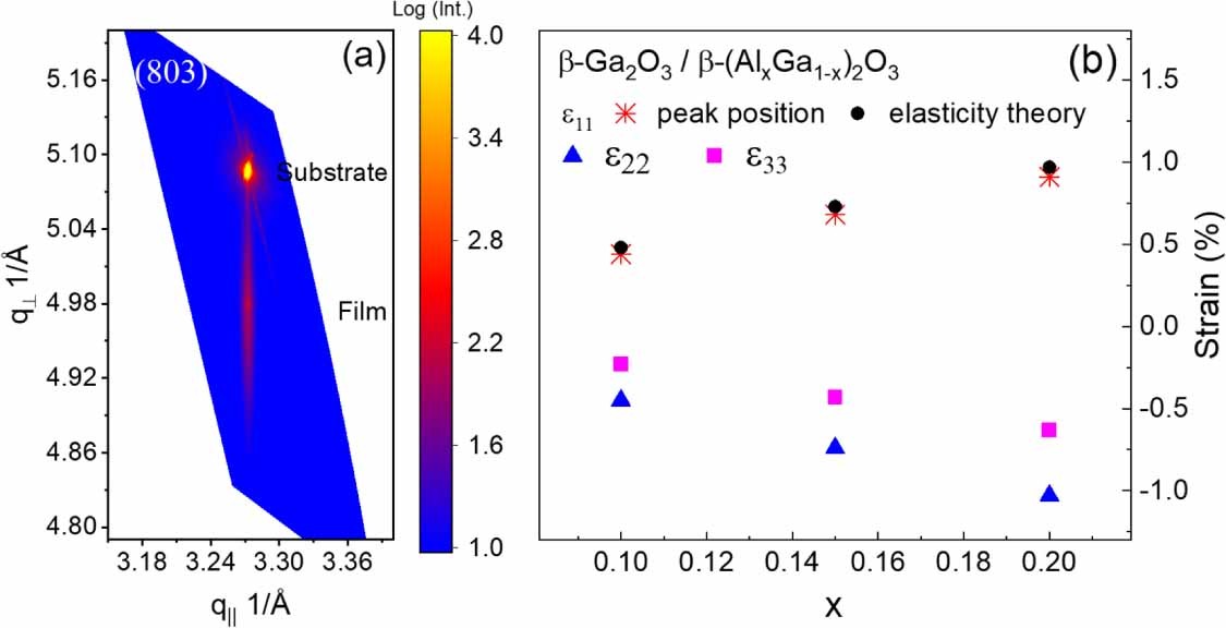
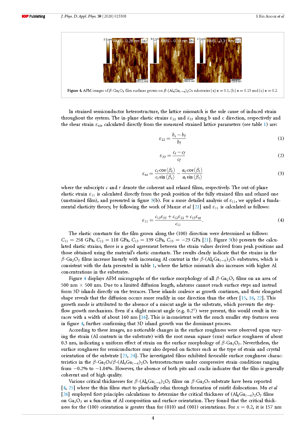
Figure 3. (a) X-ray reciprocal space maps of epitaxial β-Ga2O3 thin film (83 nm) in the vicinity of the asymmetrical (803) Bragg reflection of the β-(AlxGa1−x)2O₃ substrates x = 0.2, (b) in-plane (22 and 33 along b- and c-axis, respectively) and out-of-plane (11) normal strains versus Al composition (x) in the β-(AlxGa1−x)2O₃ substrates.
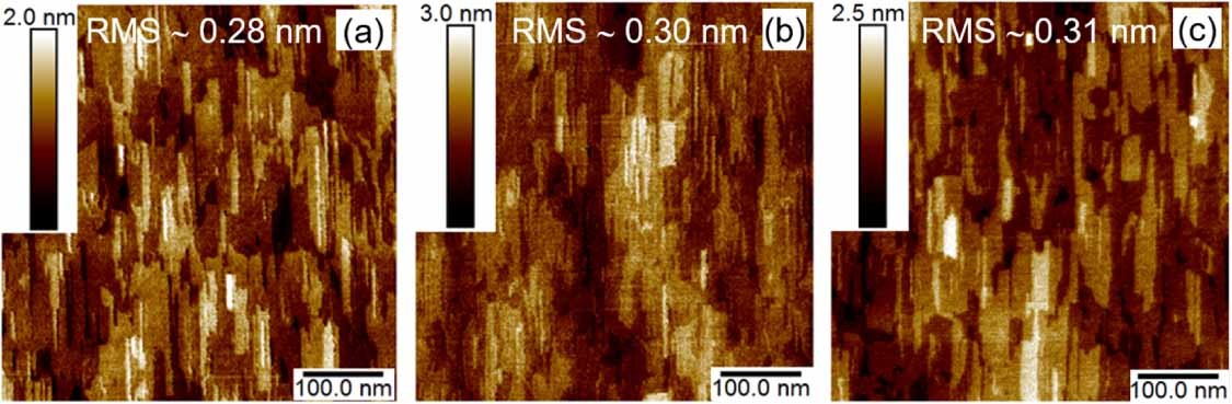
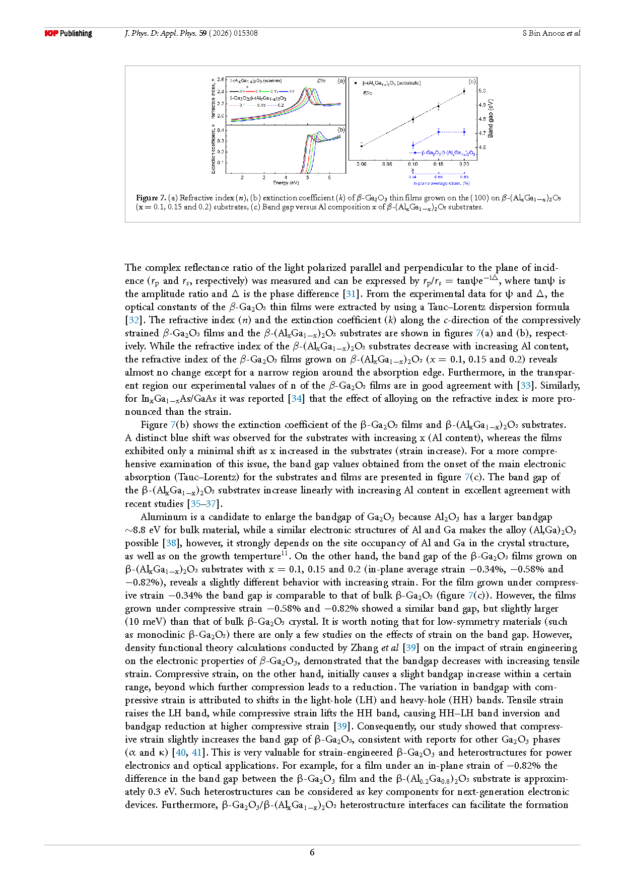
Figure 4. AFM images of β-Ga2O3 film surfaces grown on β-(AlxGa1−x)2O₃ substrates (a) x = 0.1, (b) x = 0.15 and (c) x = 0.2.
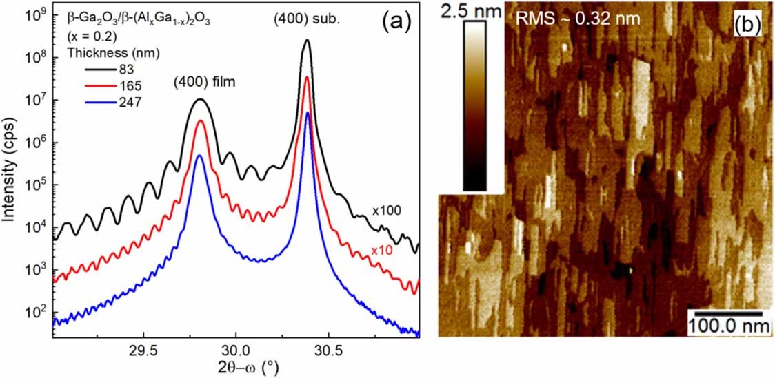
Figure 5. (a) HR-XRD 2θ–ω scans of β-Ga2O3 thin films of different thicknesses grown on β-(AlxGa1−x)2O₃ (x = 0.2) substrates, (b) AFM image, of β-Ga2O3 thin film (247 nm) grown on the (100) on β-(AlxGa1−x)2O₃ (x = 0.2) substrates.
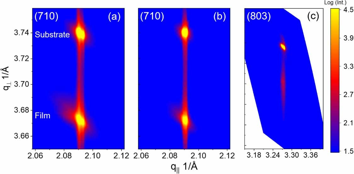
Figure 6. X-ray reciprocal space maps of epitaxial β-Ga2O3 thin film in the vicinity of the asymmetrical (710) Bragg reflection of (a) 83 nm, (b) 247 nm, and (c) in the vicinity of the asymmetrical (803) Bragg reflection of 247 nm.
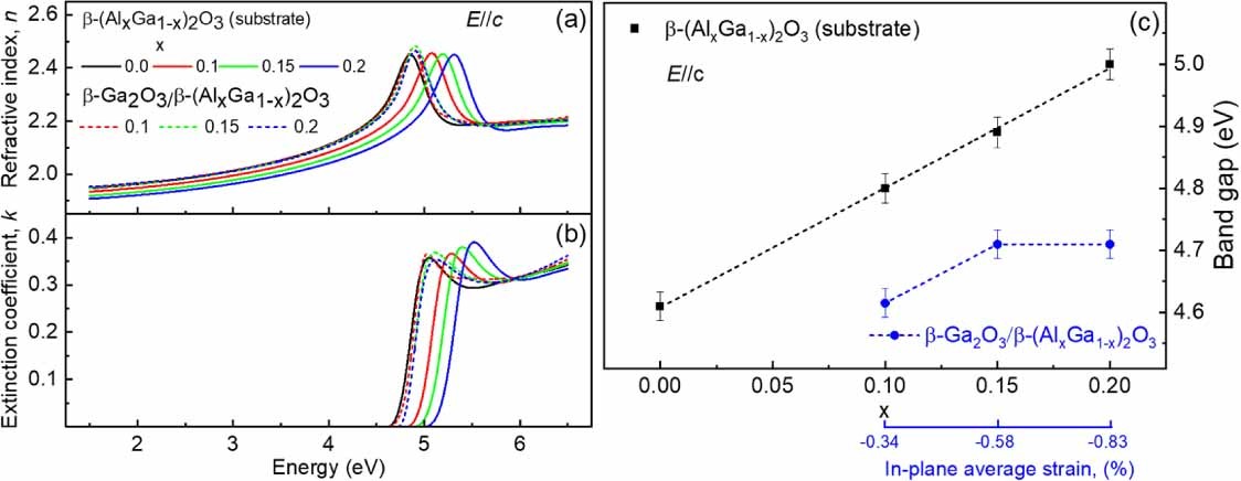
Figure 7. (a) Refractive index (n), (b) extinction coefficient (k) of β-Ga2O3 thin films grown on the (100) on β-(AlxGa1−x)2O₃ (x = 0.1, 0.15 and 0.2) substrates, (c) Band gap versus Al composition x of β-(AlxGa1−x)2O₃ substrates.
DOI:
doi.org/10.1088/1361-6463/ae2aec