Paper Sharing
【Member Papers】Thin Ga₂O₃ insertion layer for phase structure and electrical property evolutions in ferroelectric Hf₀.₅Zr₀.₅O₂ capacitors
日期:2026-01-15阅读:464
Researchers from the Fudan University have published a dissertation titled "Thin Ga2O3 insertion layer for phase structure and electrical property evolutions in ferroelectric Hf0.5Zr0.5O2 capacitors" in Applied Physics Letters.
Project Support
This work was supported in part by the National Natural Science Foundation of China under Grant Nos. 62027818 and 11974320, in part by the National Key Research and Development Program of China under Grant No. 2021YFB3202500, in part by the Atomic Layer Deposition Equipment for Third-Generation Semiconductor Power Device Fabrication (2024GXGG004), and in part by the MIND Project No. MINDXZ202402.
Background
The discovery of ferroelectricity in hafnium oxide (HfO2)-based materials in 2011 constituted a milestone achievement. Compared with conventional perovskite ferroelectrics, HfO2-based thin films exhibit notable advantages such as superior dielectric properties, robust ferroelectricity, excellent complementary metal–oxide–semiconductor (CMOS) compatibility, and outstanding scalability. These attributes make them ideal candidates for a range of microelectronic devices, including ferroelectric random-access memory (FeRAM), ferroelectric tunnel junctions (FTJs), and ferroelectric field-effect transistors (FeFETs).
Abstract
In this study, gallium oxide (Ga2O3) insertion layers (ILs) of varying thicknesses were embedded within Hf0.5Zr0.5O2 (HZO) films using atomic layer deposition (ALD). Devices with Ga2O3 ILs grown for fewer than 4 ALD Ga2O3 cycles exhibit a reduction in both remnant polarization (Pr) and coercive field (Ec). Notably, the device incorporating a IL with 2 ALD Ga2O3 cycles demonstrates strong performance, achieving a 2Pr of 47.0 μC/cm2 and an Ec of 0.92 MV/cm. In contrast, for devices with ILs exceeding 8 ALD Ga2O3 cycles, the 2Pr value remains near 18 μC/cm2, while Ec increases significantly. These divergent behaviors can be attributed to the different diffusion states of the insertion IL. For a low number of ALD Ga2O3 cycles, it is the diffusion of Ga3+ ions into the HZO region adjacent to the IL that results in a reduced Ec. Conversely, with higher ALD Ga2O3 cycles, the IL forms a continuous layer that physically divides the 10 nm HZO film into two sections, which leads to a further decrease in Pr and an increase in Ec. Furthermore, the progressive disruption of vertical grain boundaries by the growing insertion layer (IL) leads to a continuous decrease in leakage current. This work demonstrates the effective modulation of HZO devices via a Ga2O3 insertion layer, offering a methodology and data reference for enhancing device reliability.
Conclusion
In this work, the effect of a Ga2O3 IL on the ferroelectric properties of HZO thin films was systematically investigated, revealing two distinct mechanisms dependent on the IL thickness. At low ALD Ga2O3 cycles, Ga3+ diffused into the HZO film promotes t-phase formation, concurrently reducing both 2Pr and Ec. Beyond a critical thickness, however, the IL forms a continuous layer that disrupts the HZO crystal structure. This leads to a stabilized 2Pr, due to suppressed Ga3+ substitution, and a significantly increased Ec, caused by factors including, but not limited to, the voltage division effect of the interlayer and an increased density of transverse grain boundaries. The continuous decrease in leakage current with increasing IL thickness, a result of disrupted grain boundaries, contributes to improved device endurance. An optimal trade-off was achieved with 2 ALD Ga2O3 cycles, which exhibited a high 2Pr of 47.0 μC/cm2, a low Ec of 0.92 MV/cm, and endurance improved by approximately two orders of magnitude. Ultimately, this study demonstrates that Ga2O3 ILs provide an effective strategy for modulating the ferroelectric behavior of HZO, offering clear guidance for tailoring these films for diverse applications.
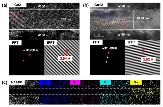
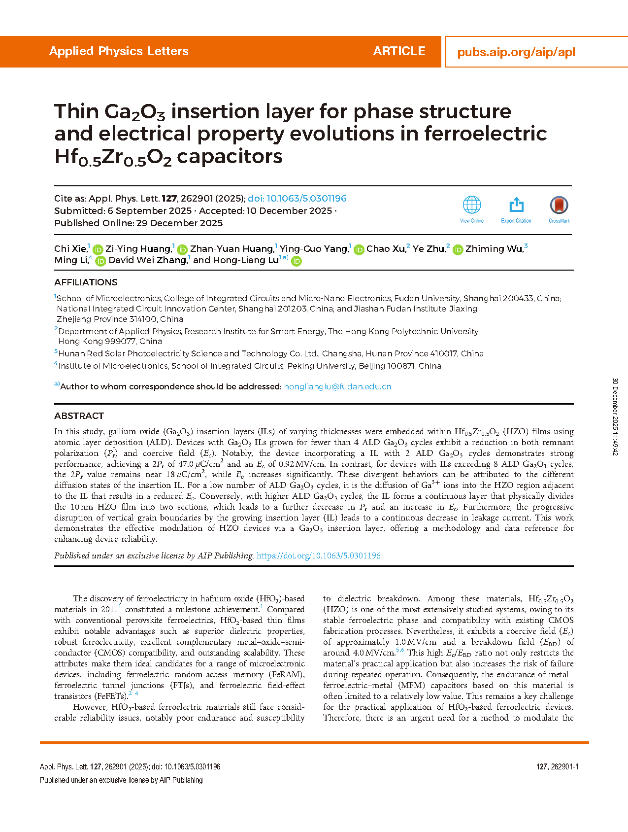
FIG. 1. (a) and (b) Cross-sectional TEM images of the Ga2 and Ga12 samples, respectively. (c) EDS elemental mapping of the ferroelectric film portion of the Ga12 sample.
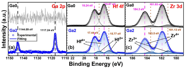
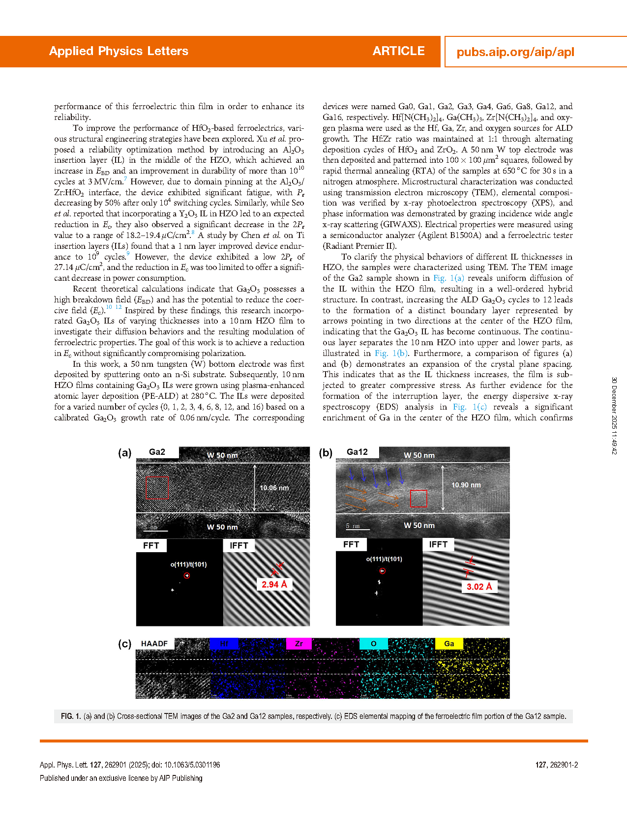
FIG. 2. The baseline subtracted XPS (a) Ga 2p, (b) Hf 4f, (c) Zr 3d spectra of Ga. The Hf 4f and Zr 3d spectra of the sample without IL are also compared.
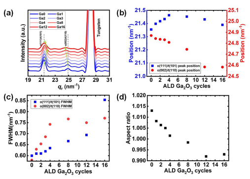
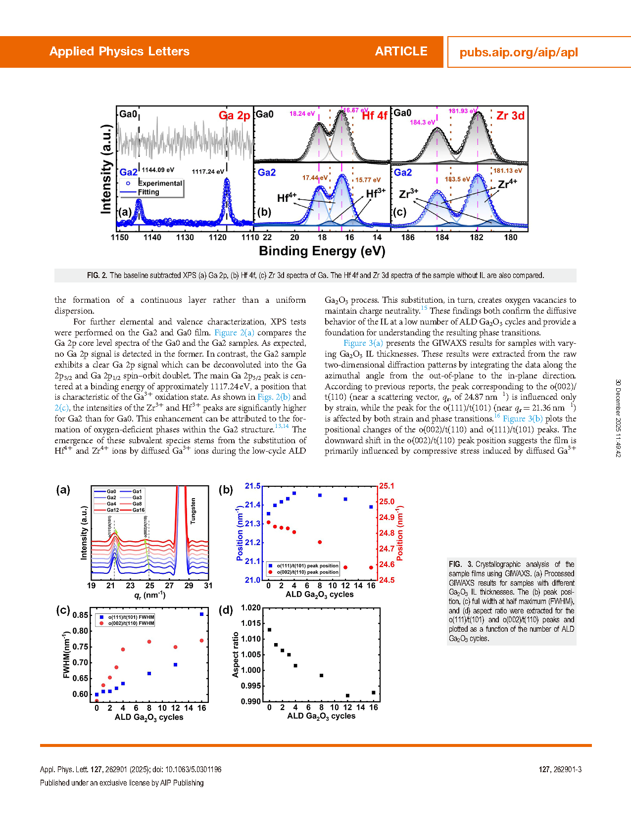
FIG. 3. Crystallographic analysis of the sample films using GIWAXS. (a) Processed GIWAXS results for samples with different Ga2O3 IL thicknesses. The (b) peak position, (c) full width at half maximum (FWHM), and (d) aspect ratio were extracted for the o(111)/t(101) and o(002)/t(110) peaks and plotted as a function of the number of ALD Ga2O3 cycles.
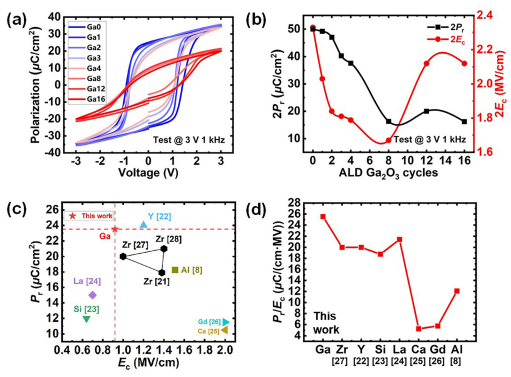
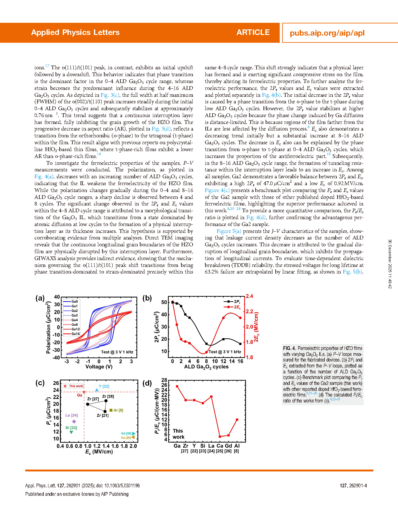
FIG. 4. Ferroelectric properties of HZO films with varying Ga2O3 ILs. (a) P–V loops measured for the fabricated devices. (b) 2Pr and Ec extracted from the P–V loops, plotted as a function of the number of ALD Ga2O3 cycles. (c) Benchmark plot comparing the Pr and Ec values of the Ga2 sample (this work) with other reported doped HfO2-based ferroelectric films. (d) The calculated Pr /Ec ratio of the works from (c).
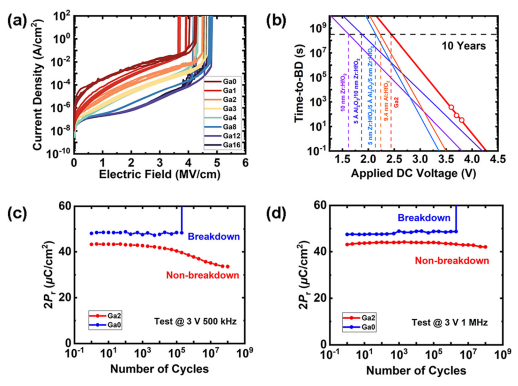
FIG. 5. (a) The TZDB characteristics of capacitors with different ALD Ga2O3 cycles. (b) Applied DC voltage extrapolation for long lifetime at 63.2% failure of the fabricated devices with different ALD Ga2O3 cycles, compared to other reported works. The endurance characteristics at (c) 500 kHz and (d) 1 MHz of Ga0 and Ga2.
DOI:
doi.org/10.1063/5.0301196