Paper Sharing
【International Papers】On the interpretation of the XRD rocking curves of heteroepitaxial Ga₂O₃ thin films grown on c-plane sapphire
日期:2026-01-16阅读:397
Researchers from the Leibniz Institute of Surface Engineering (IOM) have published a dissertation titled "On the interpretation of the XRD rocking curves of heteroepitaxial Ga2O3 thin films grown on c-plane sapphire" in Journal of Applied Physics.
Background
Ga2O3 is a promising ultra-wide bandgap semiconducting oxide with a room-temperature bandgap ranging from 4.5 to 5.3 eV, which leads to a high breakdown field strength of 8 MV/cm, making it increasingly attractive for high-power electronics and solar-blind UV-sensor applications. Another advantage of Ga2O3 as a ultra-wide bandgap semiconductor is high radiation hardness, enabling its use in harsh radiation environments.
While homoepitaxial growth on -Ga2O3 single-crystal substrates yields superior crystalline quality and carrier mobility, particular interest lies in studying heteroepitaxial growth on other substrate materials as cost-effective alternatives.
High-quality heteroepitaxial growth of Ga2O3 thin films has been achieved using a variety of chemical (CVD) and physical vapor deposition (PVD) methods. Each technique yielded specific advantages and disadvantages. For example, CVD methods such as metal organic vapor-phase epitaxy (MOVPE) enable large-area growth of high-quality thin films at the expense of high process temperature. Among PVD methods, molecular beam epitaxy (MBE) provides precise control over stoichiometry and interface quality, but at relatively low growth rates. Pulsed laser deposition (PLD) and ion beam sputter deposition (IBSD) are known as “energetic deposition” methods, with film-forming particles bringing significant kinetic energy to a growing layer, allowing for epitaxial growth at relatively low substrate temperatures (in comparison to CVD methods). However, too high particle energies may result in higher defect densities, and finding a suitable window of particle energies is necessary, which is especially important in the case of IBSD.
Abstract
The present work discusses the two-component structure of out-of-plane x-ray diffraction rocking curves (XRD RCs) of Ga2O3 thin films that are heteroepitaxially grown on c-plane sapphire substrates by ion beam sputter deposition and pulsed laser deposition. The influence of thin-film thickness, instrumental resolution, and the deposition method on the RC structure is investigated and the origins of the narrow component are discussed. It is shown that for thin Ga2O3 films on c-plane Al O , the narrow component of RCs is not an indication of high crystalline quality, but rather an effect of coherent scattering from a subset of well-aligned β-Ga2O3 domains. It was found that the variation of the narrow component intensity with the order of XRD reflection is linked to the presence of antiphase domains, and not to the contribution of the thin interfacial layer of α-Ga2O3.
Conclusions
In this study, it was shown that the two-component structure of XRD rocking curves with narrow and intense central components, of reflections from thin Ga2O3 films on c-plane sapphire, is not an indication of high crystalline quality of the whole film. The origin of the narrow peak is a result of coherent scattering from a subset of well-aligned β-Ga2O3 domains. The narrow rocking curve component is also limited by instrumental resolution. This two-component structure is not specific to IBSD-grown films and is also observed for PLD-grown Ga2O3 films, as shown in this work. Furthermore, the variation of the narrow component intensity with the order of XRD reflection (for odd–weak intensity, for even–strong intensity) is linked to the presence of antiphase domains, and not to the influence of the α-Ga2O3 layer.
Looking forward, such rocking curves with narrow components should always be carefully interpreted for heteroepitaxially grown mosaic thin films including other material/substrate systems and should not be taken as a sign of excellent crystalline quality of the whole film by itself.
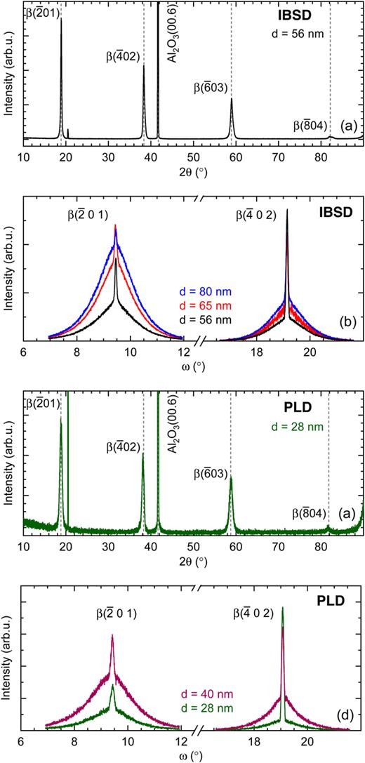
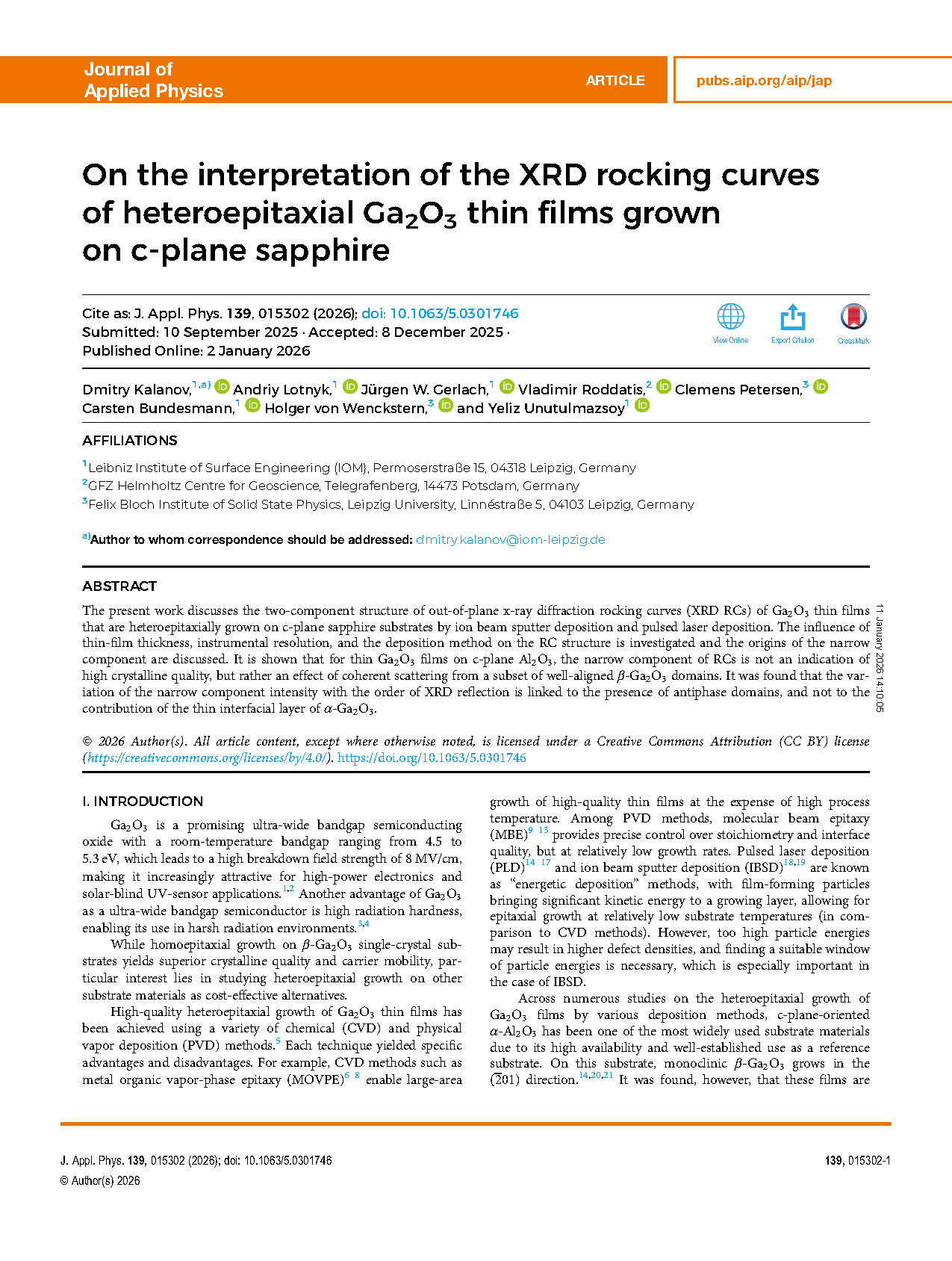
FIG. 1. XRD scans of IBSD-grown (a,b) and PLD-grown (b,c) Ga2O3 films on c-plane sapphire. (a) Out-of-plane 2θ-ω scan for a 56 nm thick IBSD-grown film. (b) Two-component -scans of β(-201) and β(-402) reflections for IBSD-grown films with thicknesses of 56, 65, and 80 nm. (c) Out-of-plane 2θ-ω scan for a 28 nm thick PLD-grown film. (d) -scans for 40 and 28 nm thick PLD-grown films.
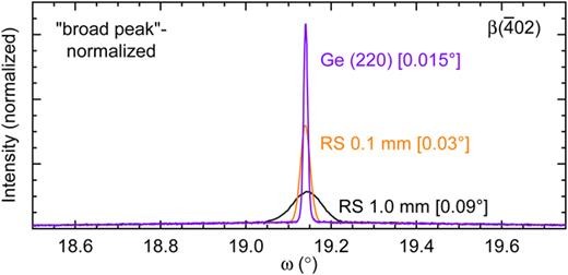
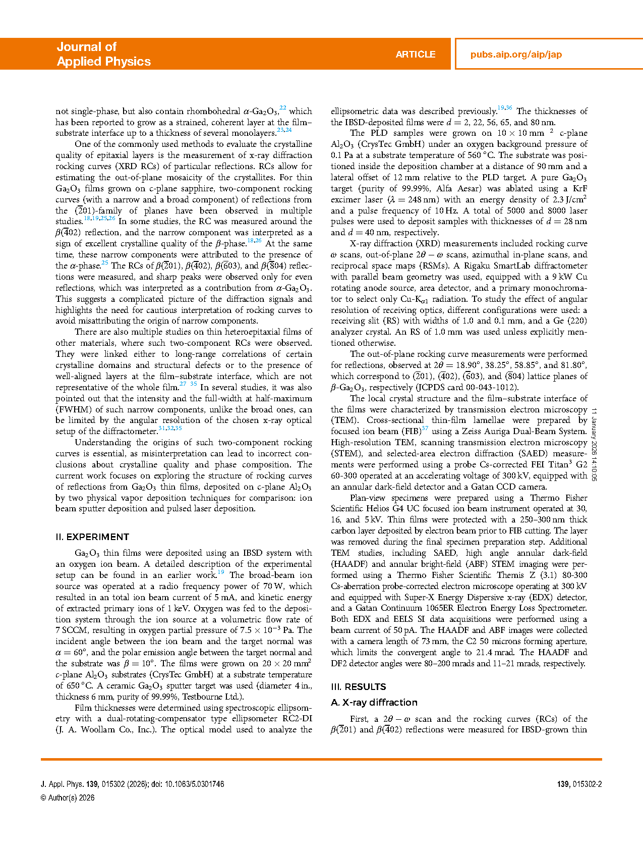
FIG. 2. Two-component ω-scans of the β(-402) reflection for an IBSD-grown 56 nm thick film in dependence on the instrumental resolution of the diffractometer. Instrumental resolution is represented by the receiving optics configuration: receiving slit (RS) of 0.1 mm, RS of 1.0 mm, or Ge (220) analyzer crystal. Corresponding FWHM values of narrow components are given in square brackets. The curves are normalized to the maximum intensity of the broad component.
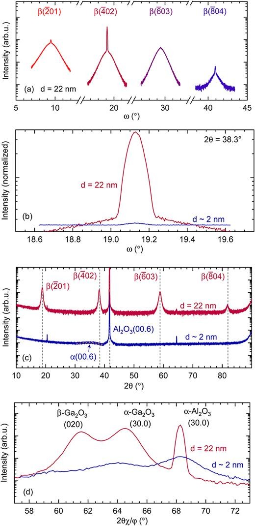
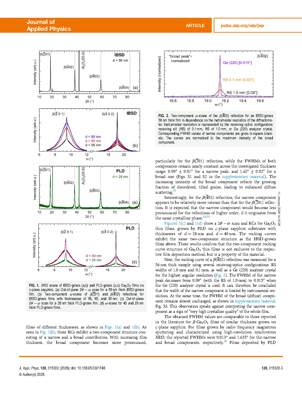
FIG. 3. XRD scans to understand the contribution of α-Ga2O3 for the 2 nm and 22 nm thick IBSD-grown films. (a) ω-scans of β(-201), β(-402), β(-603), and β(-804) reflections for a 22 nm thick film. (b) ω-scans around the β(-402) reflection, normalized by maximum intensity. (c) Out-of-plane 2θ ω scans. Dashed line marks a weak α-Ga2O3(00.6) reflection. (d) In-plane scans around β-Ga2O3(020) and α-Ga2O3(30.0) reflections.
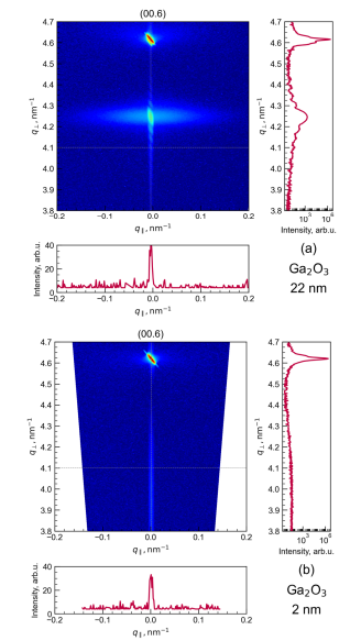
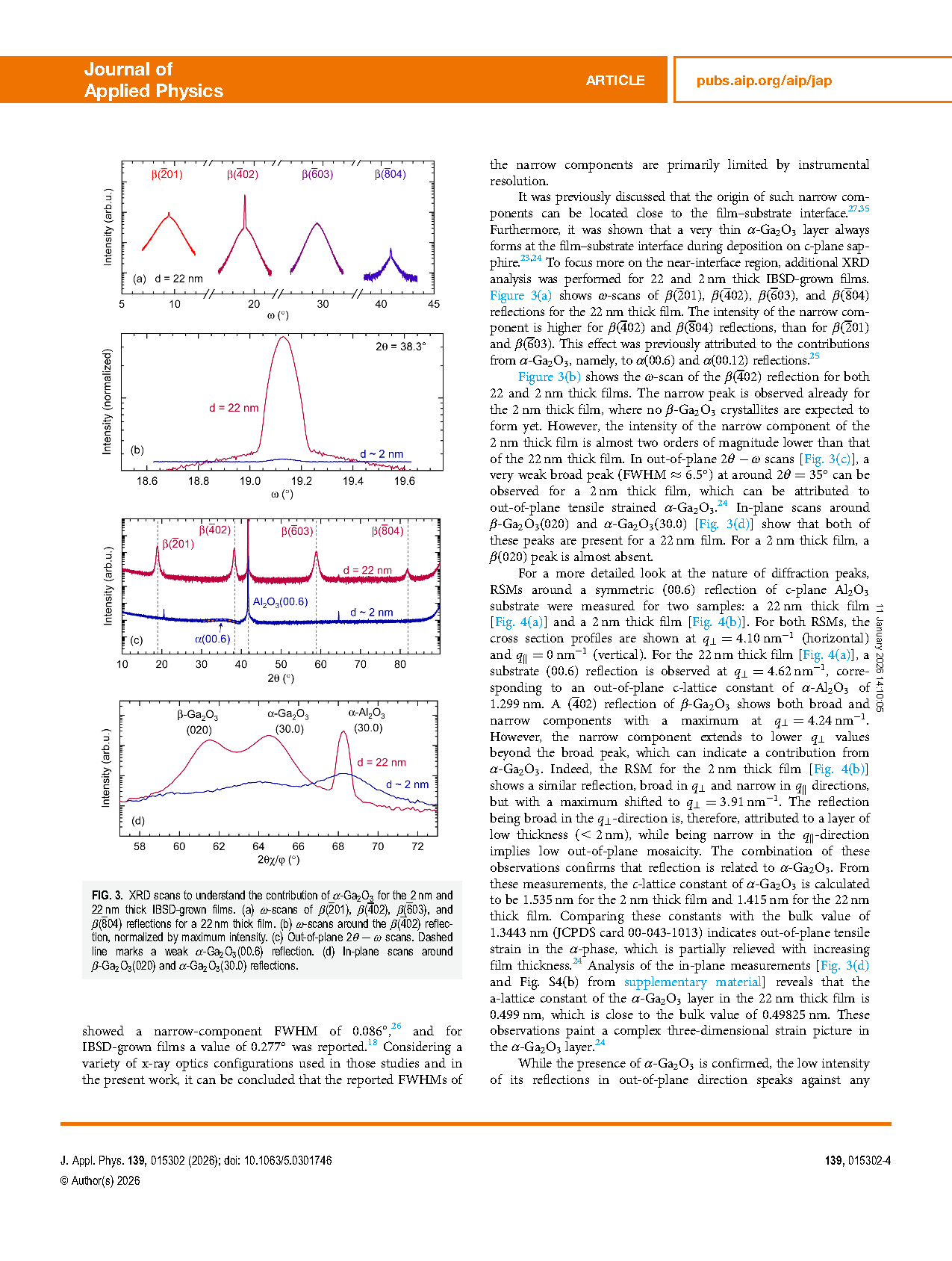
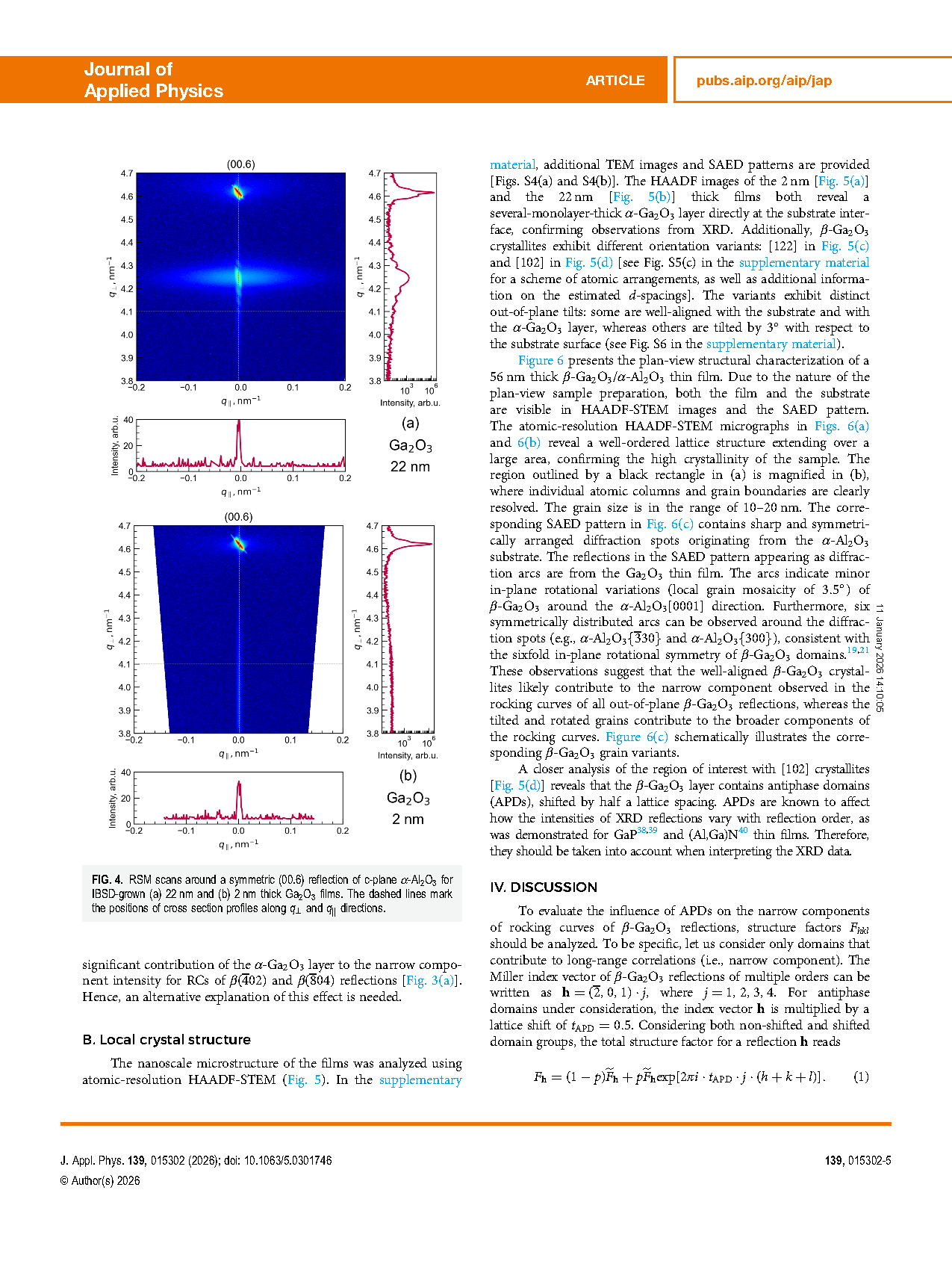
FIG. 4. RSM scans around a symmetric (00.6) reflection of c-plane α-Al2O3 for IBSD-grown (a) 22 nm and (b) 2 nm thick Ga2O3 films. The dashed lines mark the positions of cross section profiles along q⊥ and q|| directions.
DOI:
doi.org/10.1063/5.0301746