Paper Sharing
【Member Papers】Si (Mg) doping in β-Ga₂O₃ crystals by edge-defined film-fed growth: A comparative analysis of microstructure, bandgap, and temperature-dependent properties
日期:2026-01-16阅读:424
Researchers from the Guangxi University, The 46th Research Institute and Kennesaw State University have published a dissertation titled "Si (Mg) doping in β-Ga2O3 crystals by edge-defined film-fed growth: A comparative analysis of microstructure, bandgap, and temperature-dependent properties" in Journal of Crystal Growth.
Background
In recent years, β-Ga2O3 has emerged as a promising material for next-generation deep-ultraviolet optoelectronic devices and power electronic devices. Gallium oxide is an inorganic compound and ultra-wide-bandgap (UWBG) semiconductor possessing several polymorphs, among which the monoclinic β-phase, i.e., β-Ga2O3, is the most stable. β-Ga2O3 has unique advantages such as an ultra-wide band gap (up to 4.9 eV) and a high theoretical breakdown electric field strength (8 MV/cm), as well as a high Baliga figure of merit (BFOM) beyond 3,000 and more than 10 times that of SiC and GaN. In comparison with wide-bandgap (WBG) semiconductors of SiC and GaN, which are currently the most developed wide bandgap semiconductors, with commercial applications such as electric vehicle motors and desktop computer power supplies, but required complex and expensive fabrication, β-Ga2O3 can enable high-quality, large-size, low-cost, and controllably doped wafers by the melt method, showing great potential for application in power devices.
Currently, most studies on the changes in microstructure, energy band structure, etc., caused by Si doping and Mg doping have focused on a single type of doping, lacking comparative analyses between different element doping and systematic research on the influence on temperature-dependent properties. Herein, this paper employs multiple non-destructive characterization techniques such as XRD spectroscopy, photoluminescence spectroscopy, and transmission spectroscopy. By comparing the crystalline properties, defect luminescence properties, band gap properties, and temperature-dependent properties of Si-doped, Mg-doped, and unintentionally doped β-Ga2O3 single crystals, it analyzes the effects of Si doping and Mg doping on the crystal structure, band gap, and energy level structure of β-Ga2O3. Additionally, it investigates the defect luminescence properties and band gap variation properties of different doped samples under temperature-varying conditions, aiming to provide a reference for the application of doped β-Ga2O3 single crystal materials.
Abstract
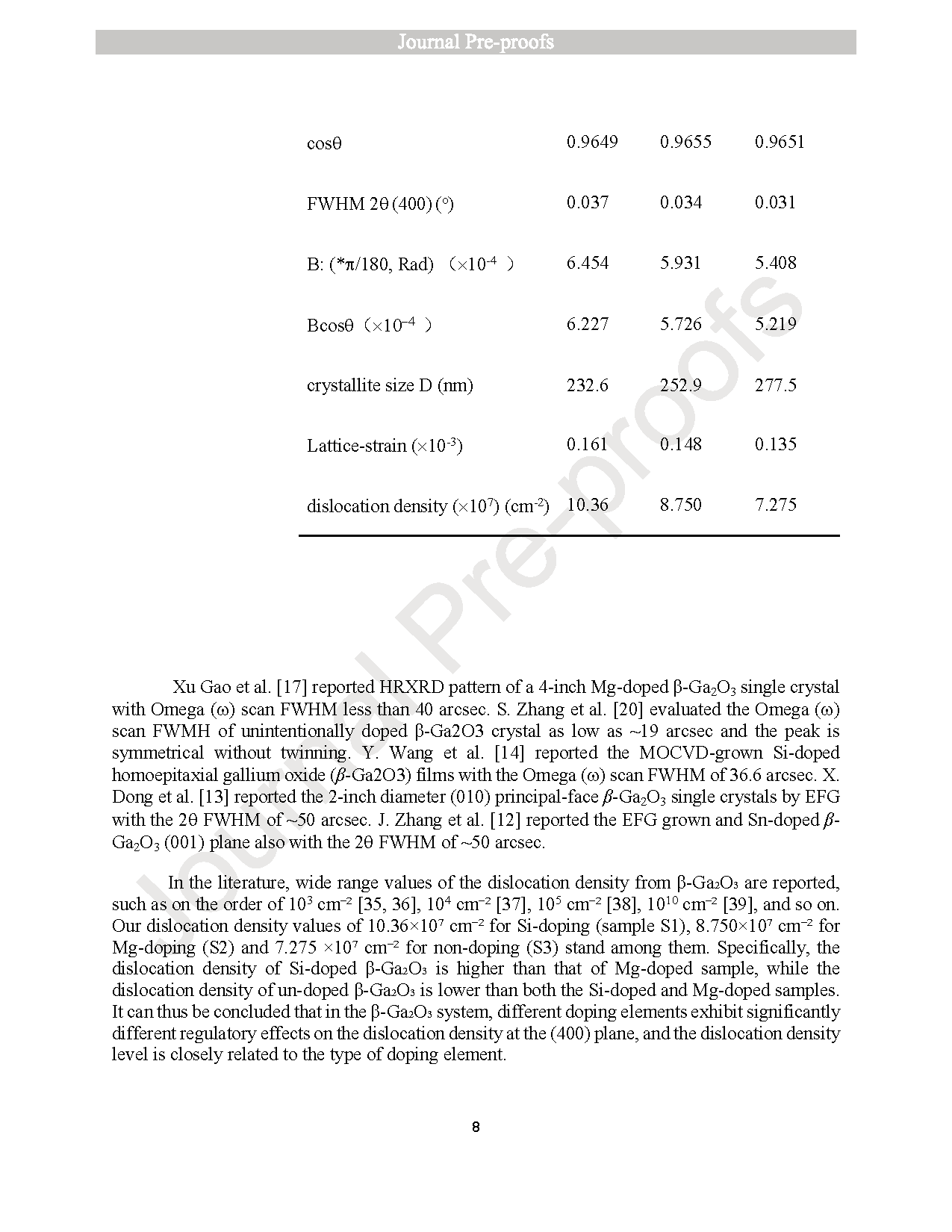
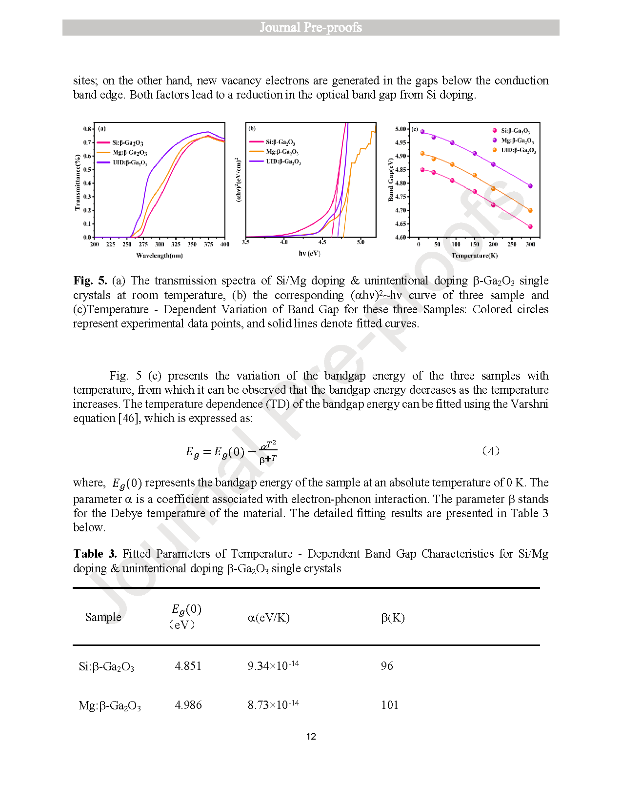
Systematic investigations of microstructure, the optical properties, band gap and variable temperature behaviors are conducted comparatively for Si/Mg-doped β-Ga2O3 crystals by edge-defined film-fed growth (EFG). The X-ray diffraction results revealed that compared with unintentionally doped β-Ga2O3 single crystals, Si doping led to a decrease in the interplanar spacing of the (400), (600), and (800) crystal planes in β-Ga2O3 single crystals, while Mg doping resulted in an increase in their interplanar spacing. Through a comprehensive analysis of the dataset of Room-temperature photoluminescence (PL), we identified that the defect-related luminescence of the two samples exhibited significantly changed. For the Si-doped sample, the PL blue emission was strong while the red emission was weak; in contrast, the Mg-doped sample showed the opposite trend, with strong red emission and weak blue emission, accompanied by multiple narrow-band red luminescence peaks. Variable-temperature photoluminescence (PL) results showed that the luminescence peak position of Si-doped β-Ga2O3 first redshifted and then blue shifted with increasing temperature, while the luminescence peak position and intensity of the Mg-doped sample exhibited a monotonous decreasing trend. Further analysis revealed that Si doping reduced the band gap, with the Fermi level moving closer to the conduction band bottom; in contrast, Mg doping increased the band gap, causing the Fermi level to shift toward the middle of the band gap. Under the variable-temperature condition from 10 K to 300 K, the temperature-dependent variation of the band gap conforms to the Varshni formula.
Highlights
● Comparison of Si/Mg doping effects on β-Ga2O3’s microstructure, bandgap, and temperature-dependent properties.
● Si doping reduces interplanar spacing, while Mg doping increases.
● Si-doped β-Ga2O3 PL peaks show unique redshift-then-blueshift with temperature, unlike Mg-doped’s monotonic shift.
● Si doping narrows the bandgap of β-Ga2O3 and Mg doping widens it.
Conclusion
In this study, the effects of Si and Mg doping on the microstructure, defect luminescence, bandgap, and temperature-dependent behavior of β-Ga2O3 single crystals were systematically compared using characterization techniques including X-ray diffraction (XRD), photoluminescence (PL), transmission spectroscopy, and ultraviolet photoelectron spectroscopy (UPS). XRD analysis showed that Si doping reduces the interplanar spacing of (400), (600), and (800) planes—due to the smaller radius of Si4+ than Ga3+ and shorter Si-O bond length. In contrast, Mg doping increases the above interplanar spacing, as Mg2+ has a larger radius than Ga3+ and longer Mg-O bond length. Room-temperature PL results revealed that the Si-doped sample exhibits strong blue emission and weak red emission, while the Mg-doped sample shows intense red emission with multiple narrow peaks — indicating that the two dopants introduce different defect energy levels. Temperature-dependent PL analysis found that the emission peak of the Si-doped sample first redshifts then blueshifts with increasing temperature, with anti-thermal quenching at 50–70 K; the Mg-doped sample shows monotonic peak blueshift and continuous luminescence intensity decrease. Optical bandgap calculations indicated that Si doping reduces the bandgap of β-Ga2O3 (to 4.63 eV), while Mg doping increases it (to 4.78 eV), both following the temperature-dependent law described by the Varshni equation. UPS measurements further confirmed that Si doping shifts the Fermi level toward the conduction band minimum (ΔEc=0.32 eV), increasing carrier concentration to 1.31×1018 cm-3 and showing n-type conductivity. In contrast, Mg doping moves the Fermi level toward the middle of the bandgap (ΔEc=1.84 eV), reducing carrier concentration and exhibiting semi-insulating behavior. This study reveals the regulation mechanisms of Si and Mg doping on the microstructure and optoelectronic properties of β-Ga2O3, providing experimental basis for the doping design of gallium oxide-based power and optoelectronic devices.
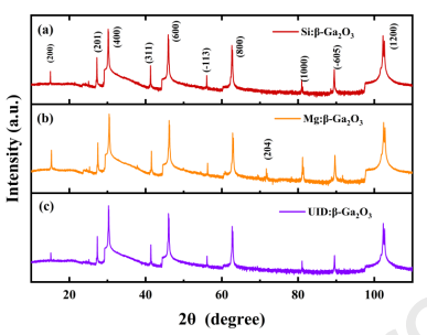
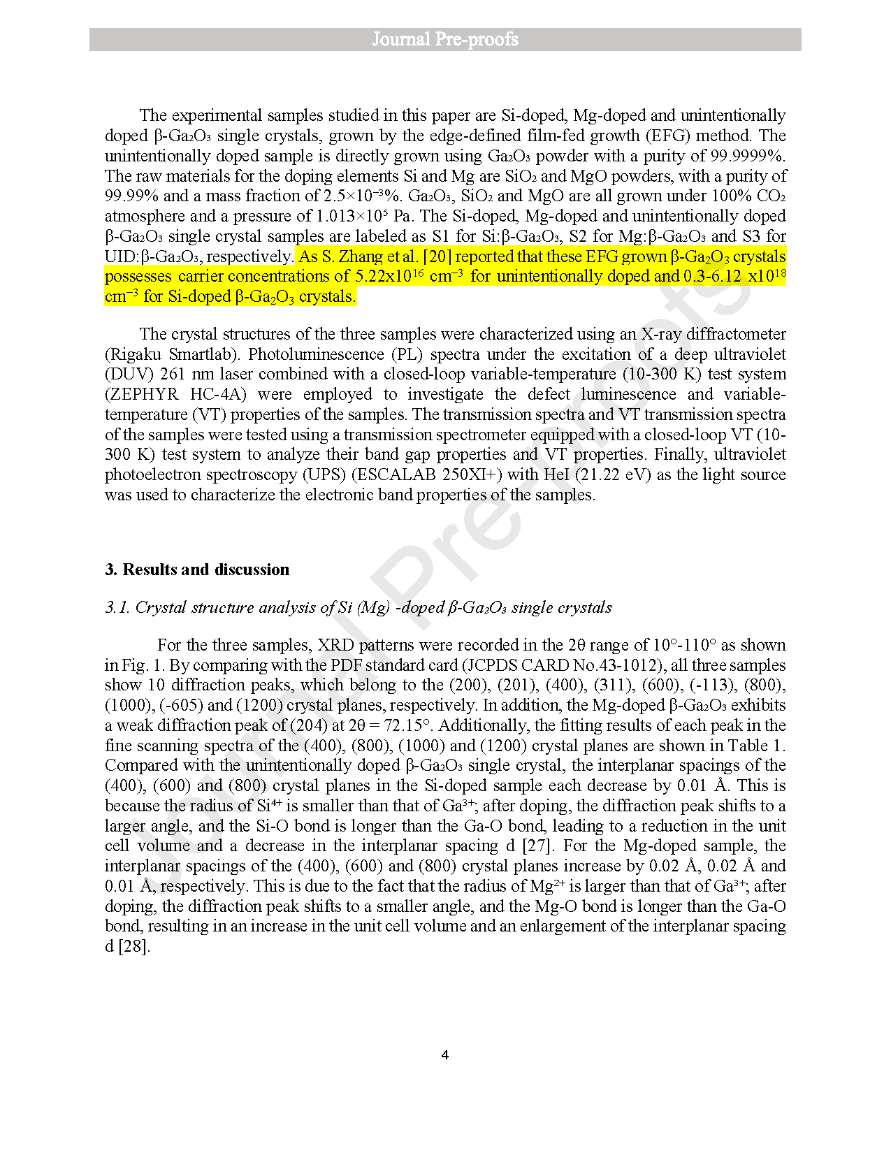
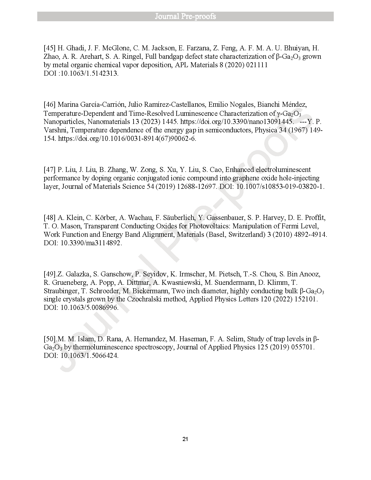
Fig. 1. X-ray diffraction(XRD)patterns of Si-doped (a), Mg-doped (b), and unintentionally doped (c) β-Ga2O3 single crystals, grown by the edge-defined film-fed growth (EFG) method.
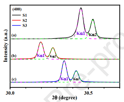
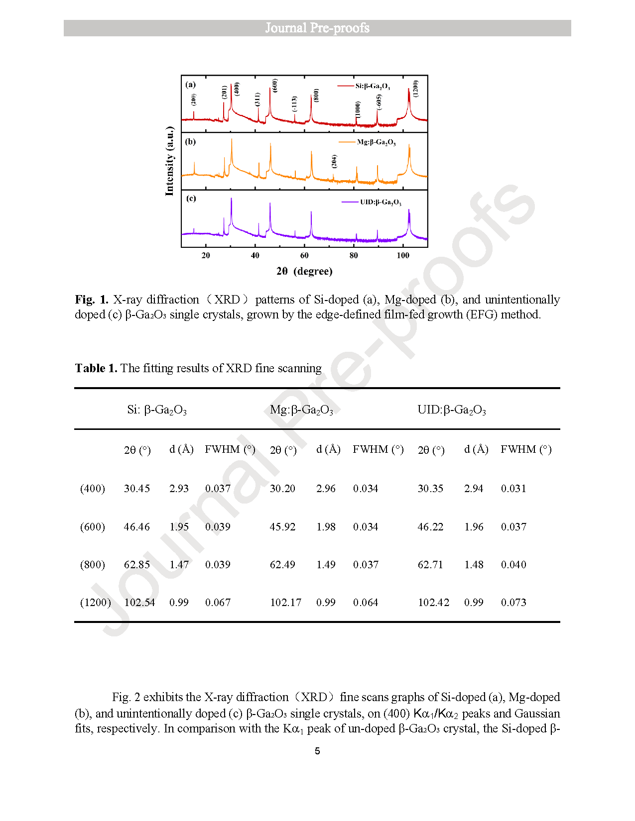
Fig. 2. X-ray diffraction(XRD)fine scans of Si-doped (a), Mg-doped (b), and unintentionally doped (c) β-Ga2O3 single crystals, on (400) peaks and Gaussian fits.
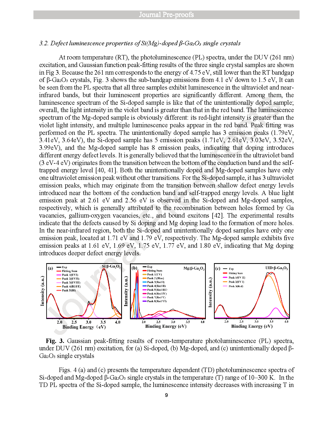
Fig. 3. Gaussian peak-fitting results of room-temperature photoluminescence (PL) spectra, under DUV (261 nm) excitation, for (a) Si-doped, (b) Mg-doped, and (c) unintentionally doped β-Ga2O3 single crystals.
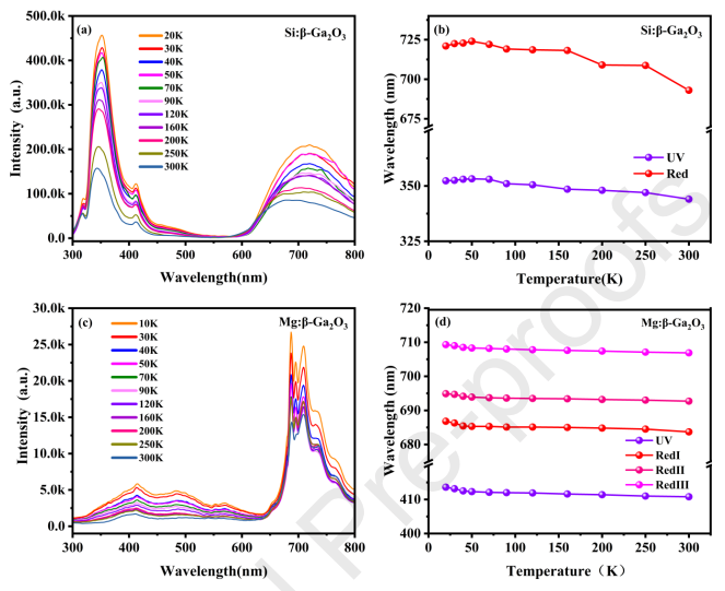
Fig. 4. (a), (c) Variable temperature PL spectrum measurement of Si doping and Mg doping β-Ga2O3 and (b), (d) the schematic diagram of luminous peak position changing with temperature, respectively.
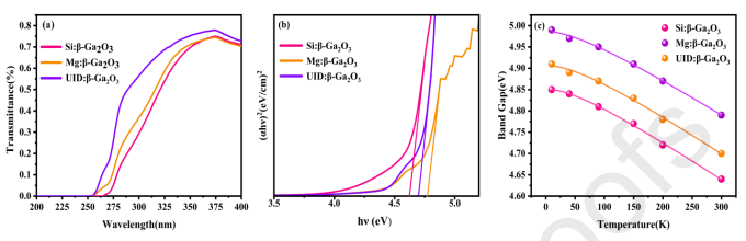
Fig. 5. (a) The transmission spectra of Si/Mg doping & unintentional doping b-Ga2O3 single crystals at room temperature, (b) the corresponding (ahn)2~hn curve of three sample and (c)Temperature - Dependent Variation of Band Gap for these three Samples: Colored circles represent experimental data points, and solid lines denote fitted curves.
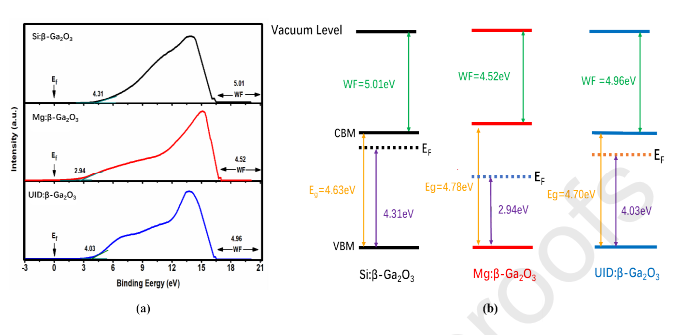
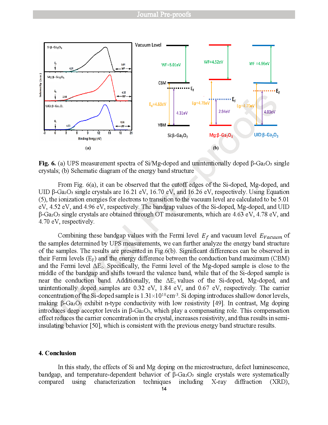
Fig. 6. (a) UPS measurement spectra of Si/Mg-doped and unintentionally doped β-Ga2O3 single crystals; (b) Schematic diagram of the energy band structure.
DOI:
doi.org/10.1016/j.jcrysgro.2026.128487