Paper Sharing
【Member Papers】MOCVD-grown α-Ga₂O₃ with increased growth rate and improved crystal quality for deep UV optoelectronics application
日期:2026-01-20阅读:429
Researchers from the Northeast Normal University have published a dissertation titled "MOCVD-grown α-Ga2O3 with increased growth rate and improved crystal quality for deep UV optoelectronics application" in Applied Physics Reviews.
Background
Ultra-wide bandgap (UWBG) semiconductor materials are indispensable for solar-blind ultraviolet (UV) photodetection applications. Although the monoclinic β-Ga₂O₃ phase is the most stable and extensively studied, the corundum-structured α-Ga₂O₃ offers certain advantages. Its wider bandgap enables more precise cutoff characteristics for deep-UV light. α-Ga₂O₃ shares the same crystal structure (corundum) as the commonly used sapphire (Al₂O₃) substrates, making high-quality heteroepitaxial growth theoretically easier and offering better compatibility with existing GaN-based optoelectronic processes. However, α-Ga₂O₃ is a metastable phase. Under conventional epitaxial growth conditions, it readily transforms into the β phase at high temperatures. To maintain the α phase, growth is typically conducted at relatively low temperatures. Low-temperature growth, however, leads to incomplete precursor decomposition, resulting in extremely low growth rates and poor crystal quality. Slow growth rates not only increase production costs but also limit the development of thick-film devices, while poor crystal quality directly causes slow detector response and high dark current. This study proposes a novel growth strategy aimed at simultaneously overcoming the trade-offs among phase stability, growth rate, and crystal quality.
Abstract
α-Ga2O3 films with a more than threefold increase in growth rate were epitaxially grown on m-Al2O3 at 530 °C by employing a 700 °C high-temperature buffer layer (HTBL) in metal–organic chemical vapor deposition growth. The underlying mechanism of the enhanced growth was understood experimentally by the surface analysis and theoretically by a model based on Gibbs–Thomson equation and first-principles calculations. With HTBL, the crystal quality of the α-Ga2O3 was also significantly improved, as evidenced by the decreased x-ray diffraction rocking curve linewidth of the (30-30) peak. The linewidth is down to 0.387°, which is significantly narrower than 0.592° from sample without HTBL. The surface morphology of HTBL features larger, more sparsely distributed islands, resulting in a lower chemical potential on the surface, which promotes the adsorption of Ga2O3-clusters by reducing the desorption and thus increases the growth. x-ray photoelectron spectroscopy showed more oxygen vacancies (Vo) on the HTBL surface. First-principles calculations indicated that Vo in the (30-30)-surface reduced the adsorption energy from −5.48 to −6.61 eV, thereby promoting cluster adsorption. A solar-blind ultraviolet photodetector based-on α-Ga2O3 exhibited an ultra-low dark current of 0.1 pA at 10 V, a high light-to-dark current ratio of 106, a responsivity of 0.54 A/W, and a detectivity of 5.5 × 10¹² Jones.
Conclusion
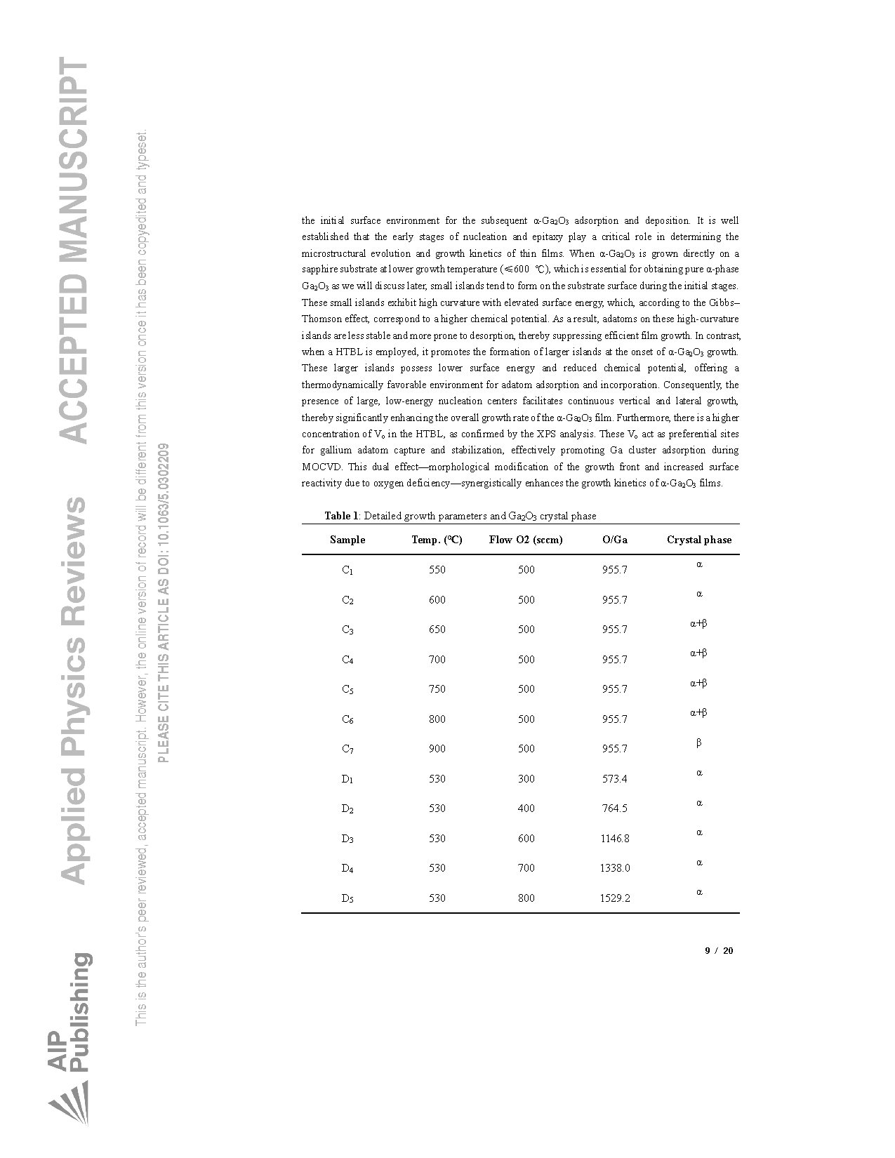
In summary, pure phase α-Ga2O3 thin films were successfully epitaxially grown on m-plane sapphire substrates via the MOCVD method. By introducing a HTBL, the crystalline quality of the α-Ga2O3 films was significantly improved, as evidenced by a reduction in the full width at half maximum (FWHM) of the (30-30) XRD rocking curve from 0.592° to 0.417°. Simultaneously, the film growth rate increased markedly from 1.56 ± 0.05 nm/min (mean ± standard deviation) to 5.38 ± 0.10 nm/min (mean ± standard deviation), demonstrating the effectiveness of the buffer layer strategy in enhancing both film quality and deposition efficiency. Further optimization of the growth parameters led to an even narrower FWHM of 0.387°, indicating superior crystallinity. Based on this high-quality film, a metal – semiconductor–metal (MSM) structured solar-blind ultraviolet photodetector was fabricated using thermally evaporated interdigital Al electrodes. The resulting device exhibited excellent performance, including an ultra-low dark current of 0.1 pA under a 10 V bias, a high photo-to-dark current ratio of 106 , a peak responsivity of 0.54 A/W, and a detectivity of 5.5 × 10¹² Jones. Notably, under low-light conditions (0.52 μW/cm2), the photodetector maintained a responsivity of 16 mA/W and a detectivity of 1.62 × 10¹¹ Jones, highlighting its potential for high-sensitivity DUV detection in low-intensity environments. These results demonstrate that the combined use of HTBL and optimized growth conditions offers a viable pathway toward the scalable fabrication of high-performance α-Ga2O3-based solar-blind photodetectors.
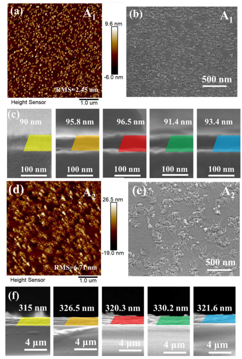
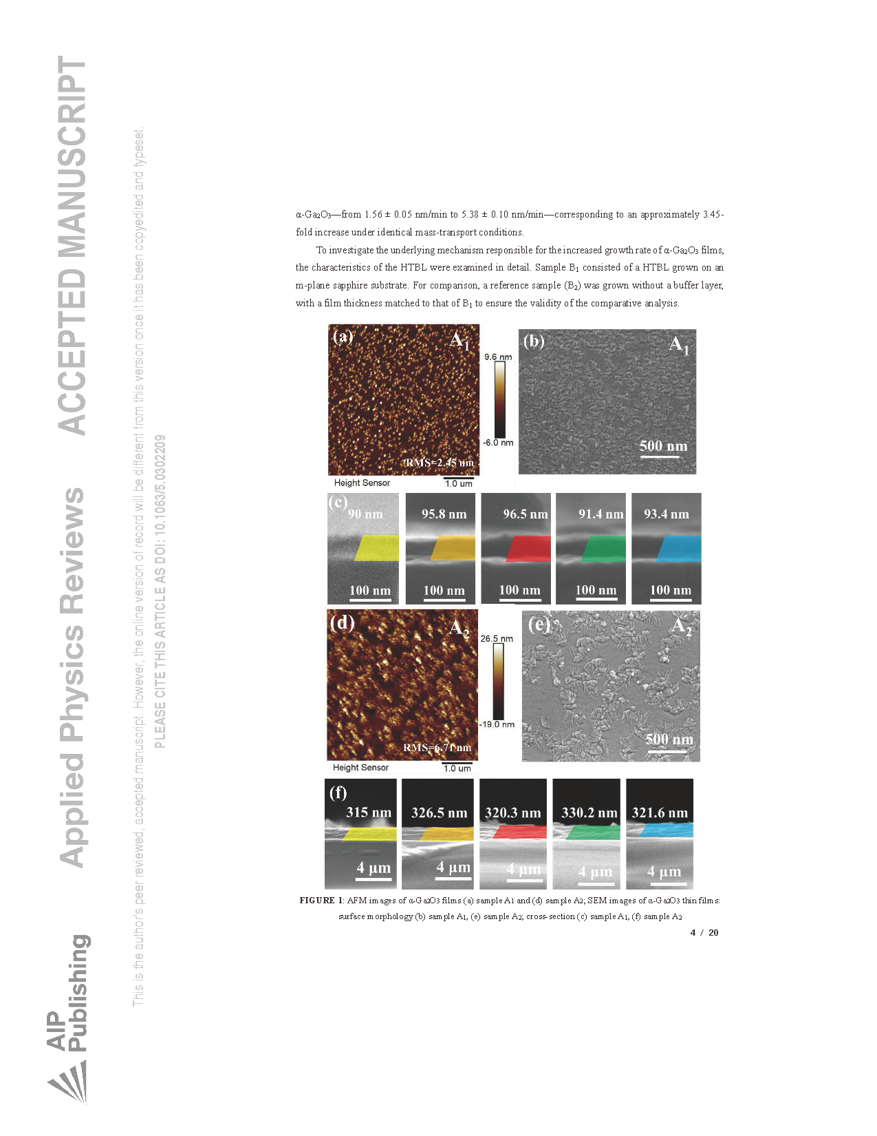
FIGURE 1: AFM images of α-Ga2O3 films (a) sample A1 and (d) sample A2; SEM images of α-Ga2O3 thin films: surface morphology (b) sample A1, (e) sample A2; cross-section (c) sample A1, (f) sample A2
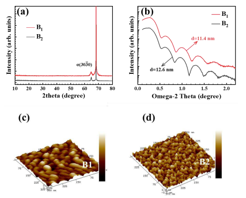
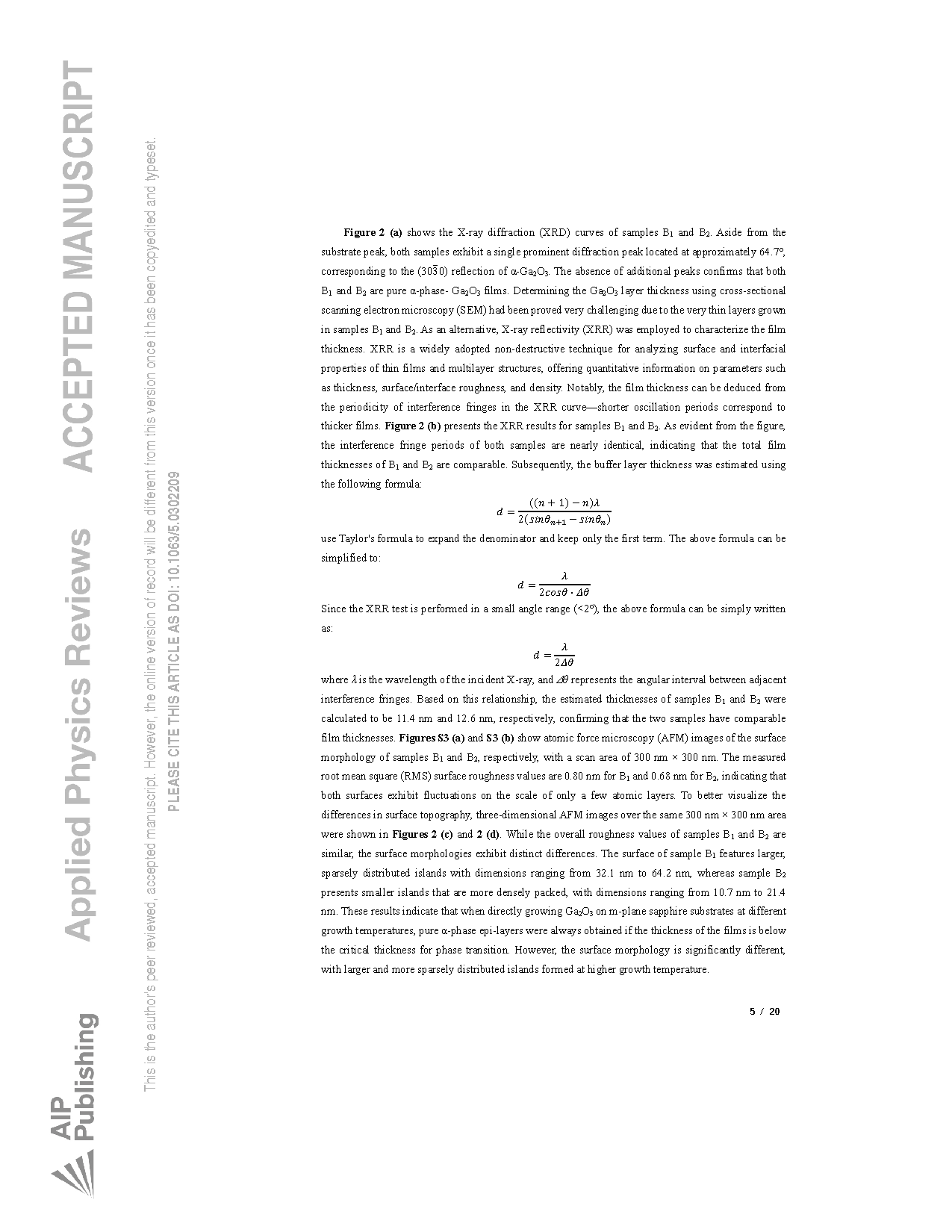
FIGURE 2: (a) XRD curves of samples B1 and B2; (b) XRR curves of samples B1 and B2; (c) 3D surface morphology of sample B1 and (d) sample B2, the scanning range is 300 nm ×300 nm
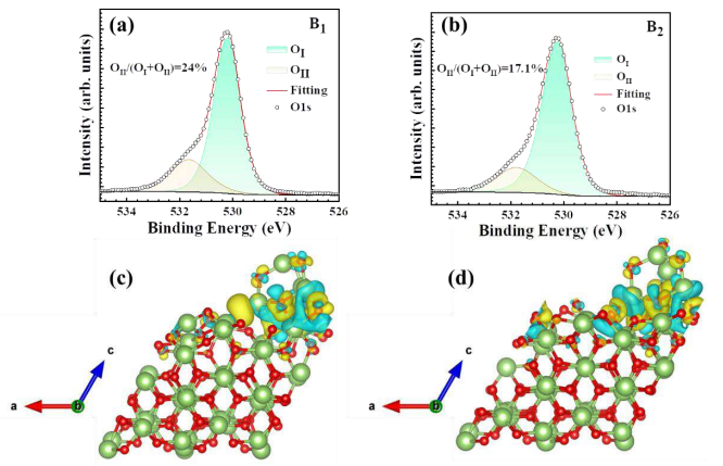
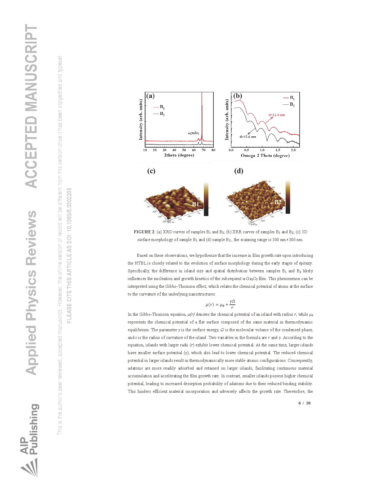
FIGURE 3: the XPS O1s spectra of (a) samples B1 and (b) sample B2, respectively; charge density difference on the surface of α-Ga2O3 (c) with Vo (d) without Vo.
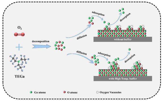
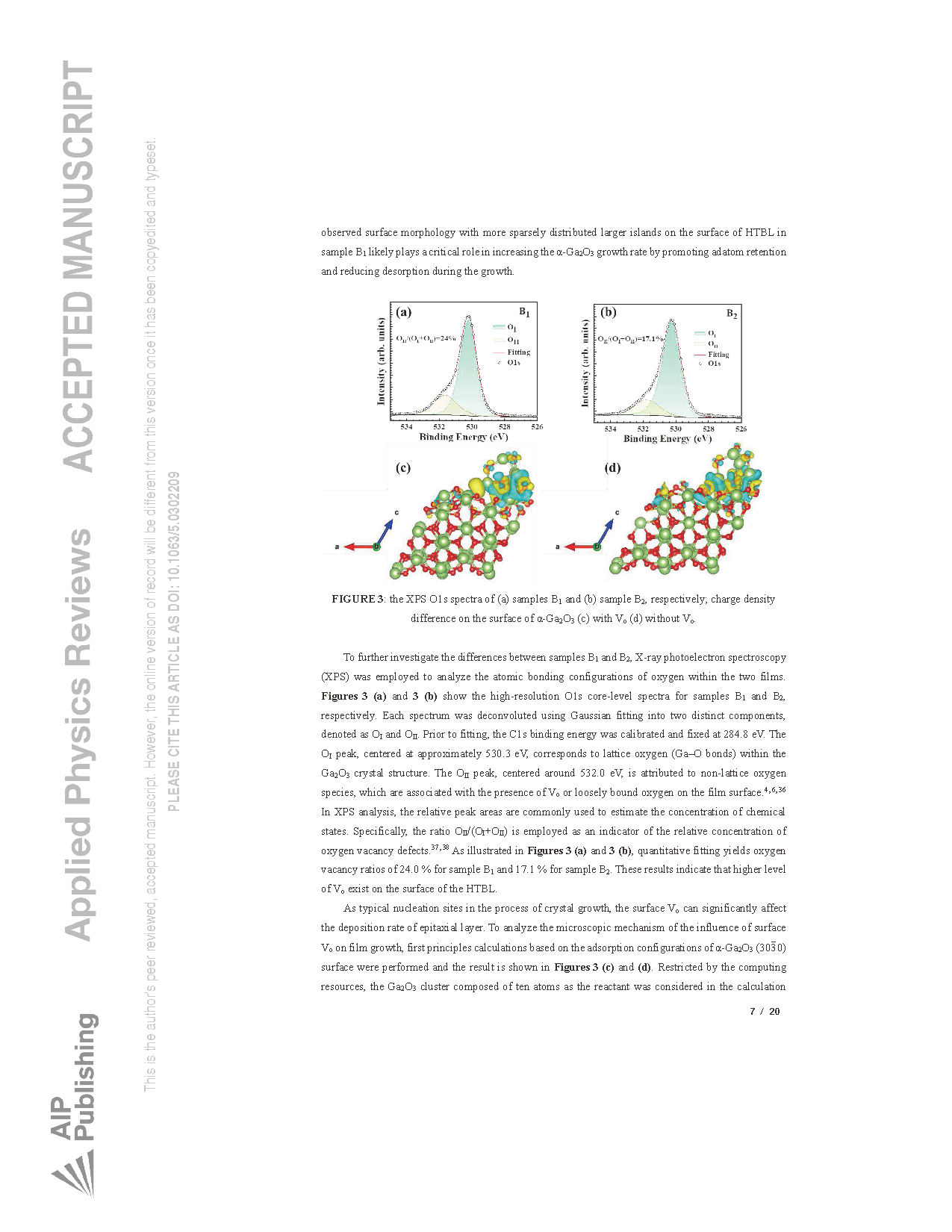
FIGURE 4: Schematic diagram of the effect of high temperature buffer layer on growth rate.
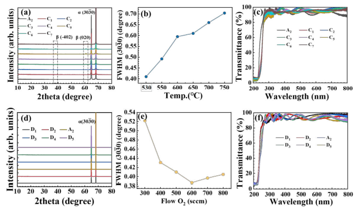
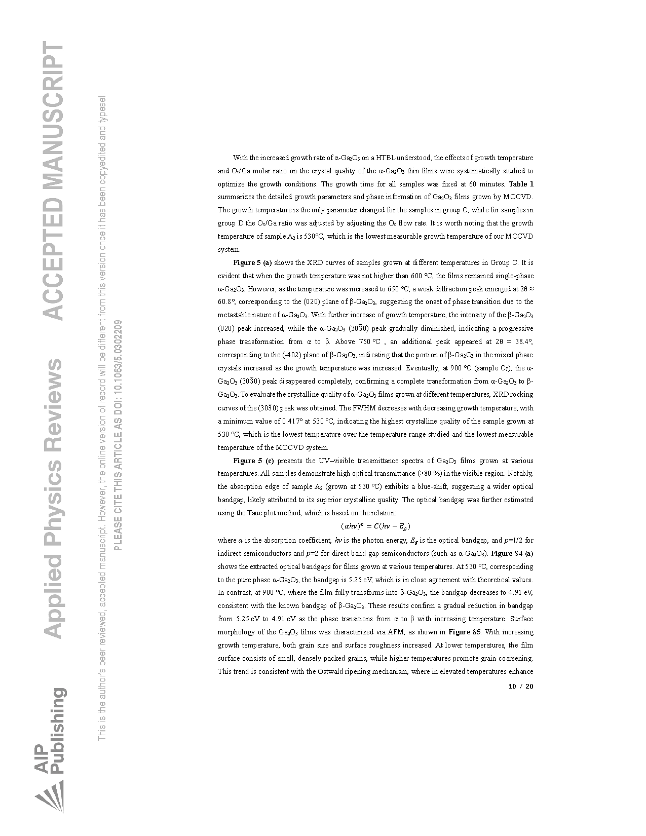
FIGURE 5: (a) XRD patterns of Ga2O3 grown at different growth temperatures; (b) FWHM of the (30-30) peak changing with growth temperature; (c) Transmission spectra of Ga2O3 grown at different growth temperatures; (d) XRD patterns of Ga2O3 grown under different O/Ga ratios; (e) FWHM of (30-30) peak changing with O/Ga ratio; (f) Transmission spectra of Ga2O3 with different O/Ga ratios atomic diffusion, leading to the dissolution of smaller islands and their incorporation into larger ones.
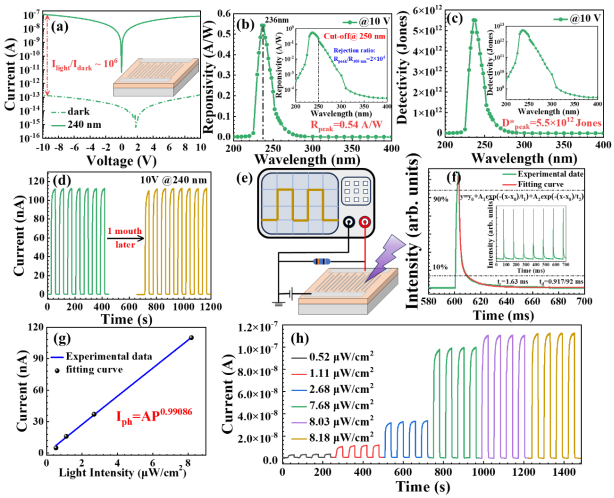
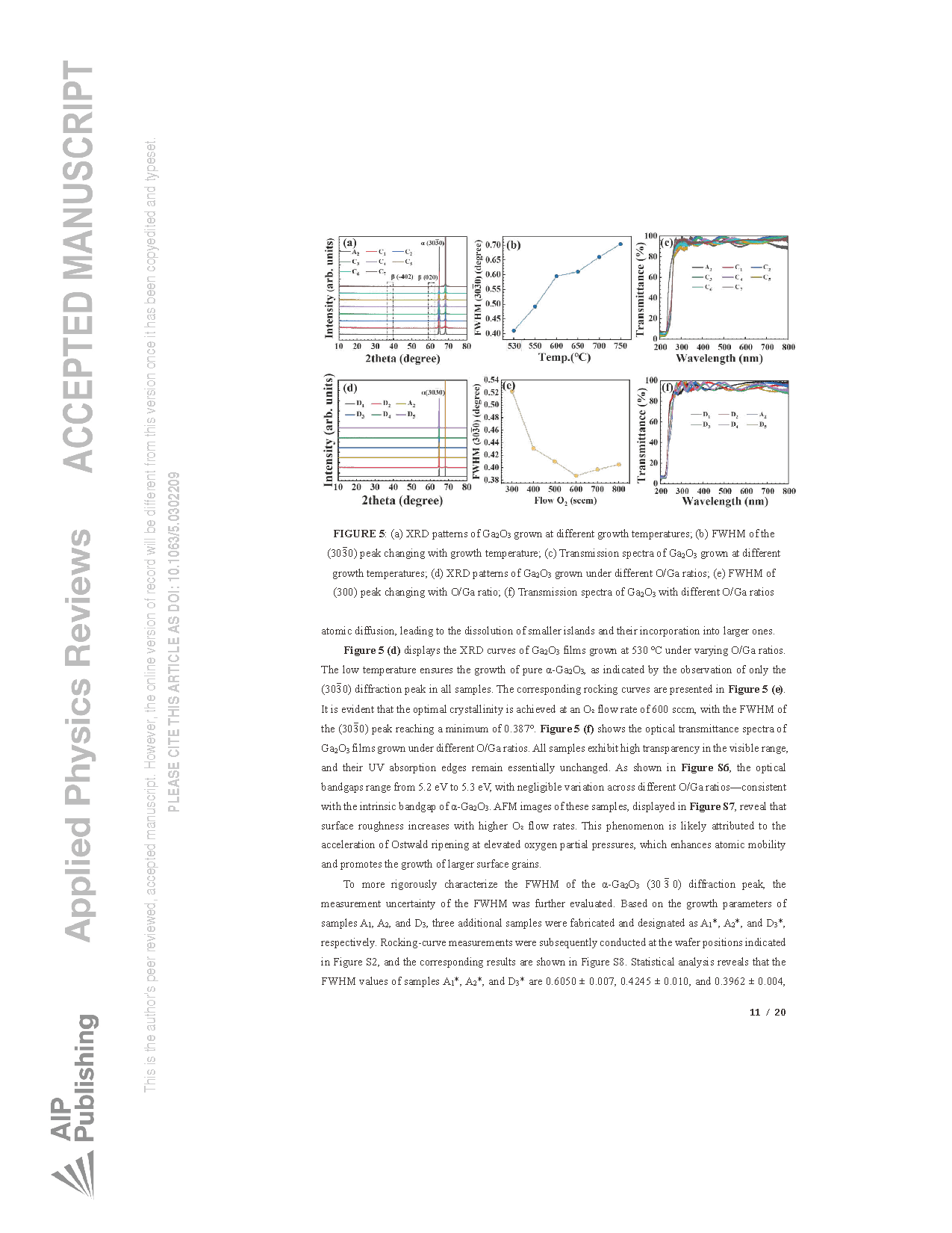
FIGURE 6: (a) Typical I-V characteristic curves of the device in the dark and under 240nm light, and the inset is a schematic diagram of the device structure; Under 10V bias, the device's responsivity spectrum at different wavelengths (b), detectivity spectrum (c), and the inset are all displayed on logarithmic coordinates; (d) I-t curve of the device under 10V bias and 240nm light illumination; (e)Schematic diagram of the device’s photo-response measurement configuration; (f) Time-resolved response of the device photocurrent at 10 V, and the inset is a magnified view of the single-pulse optical response at 10 V bias; (g) Relationship between photocurrent and light intensity at 10 V bias under 240 nm illumination fitted by power law formula; (g) The relationship between the photocurrent and light intensity at a bias voltage of 10 V under 240 nm illumination fitted by the power law formula; (h) The I-t cycle curve of the device under different light intensities when the incident light wavelength is 240 nm.
DOI:
doi.org/10.1063/5.0302209