Paper Sharing
【Domestic Papers】Achieving high carrier concentration β-Ga₂O₃ epilayers via MOCVD using SiCl₄ as dopant
日期:2026-01-20阅读:468
Researchers from the Fuzhou University have published a dissertation titled "Achieving high carrier concentration β-Ga2O3 epilayers via MOCVD using SiCl4 as dopant" in Applied Physics Letters.
Background
β-Ga₂O₃ is an ultra-wide-bandgap semiconductor with great potential for high-performance power electronics and solar-blind ultraviolet photodetectors, particularly due to its high Baliga figure of merit and the availability of large-area single-crystal substrates. For practical devices, transparent conductive electrodes and low-resistance ohmic contact layers require epilayers with simultaneously high carrier concentration and high electron mobility. However, on the (100) plane—currently the only orientation suitable for large-scale industrial substrate production—electron mobility degrades severely at high doping levels, limiting device performance. This challenge arises from anisotropic crystal properties, dopant-related scattering, defect formation, and unintentional impurity contamination. Although in-situ Si doping via conventional precursors such as SiH₄ has been widely used, maintaining high mobility at high carrier concentrations remains difficult. Therefore, developing new doping strategies and epitaxial approaches that enable high-quality, highly conductive (100)-oriented β-Ga₂O₃ epilayers is a critical step toward low-cost, scalable Ga₂O₃ device technologies.
Abstract
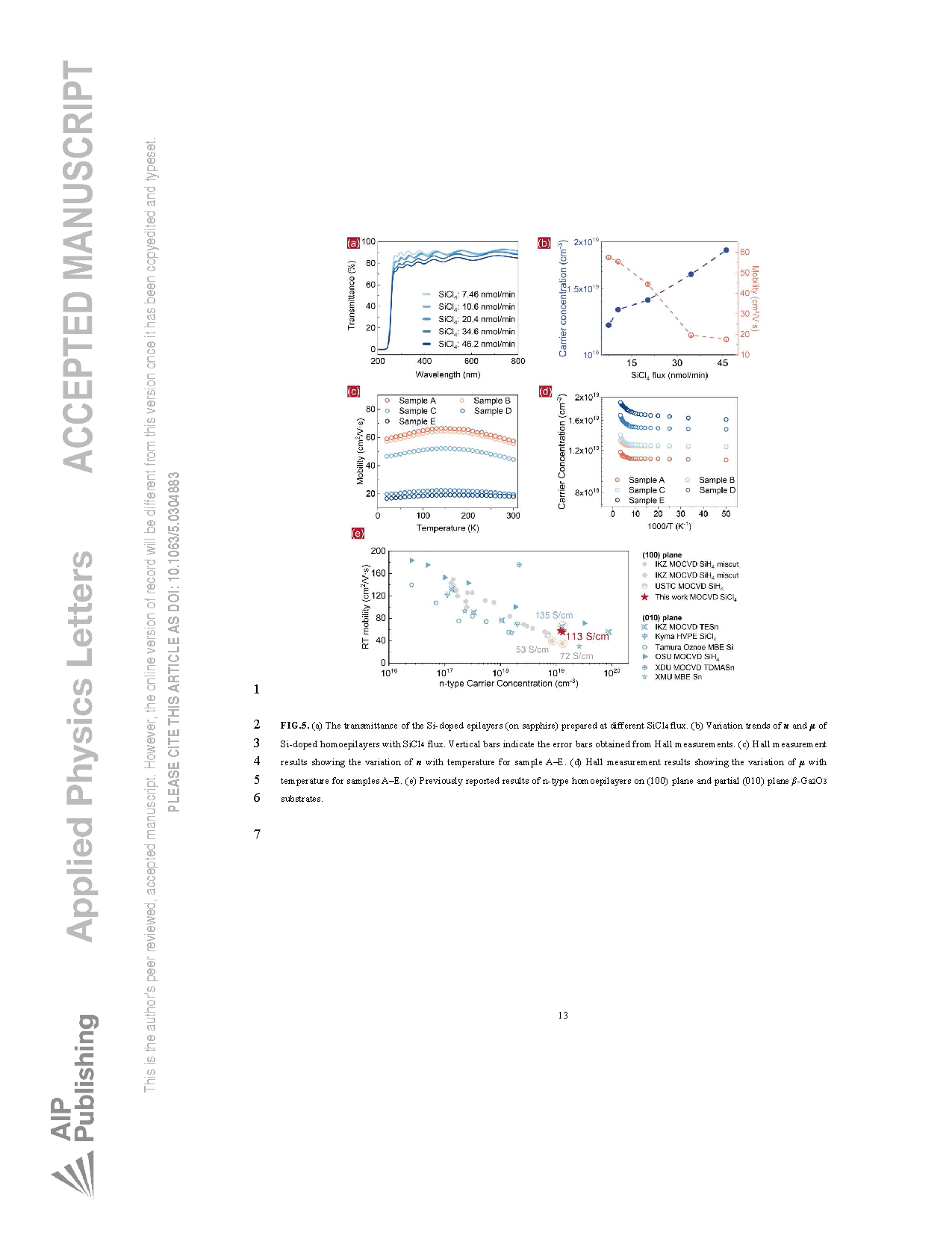
Gallium oxide (Ga₂O₃) transparent conductive electrodes and power-device contact layers are critical components for Ga₂O₃-based electronics. However, the intrinsically low electron mobility (μ) of the (100) plane, which is preferred for large-scale substrate production, under high carrier concentration (n) has hindered device performance and practical deployment. To overcome this bottleneck, we employed unintentionally miscut (100) substrates and optimized thermal and kinetic conditions to achieve step-flow homoepitaxy with ideal surface morphology. Following the elimination of surface Si contamination, in-situ Si doping was performed utilizing silicon tetrachloride (SiCl₄). SiCl₄ proved highly effective for fabricating high-n homoepilayers, yielding films with high crystalline quality, low surface roughness, and more than 80% optical transmittance in the 260–800 nm range. Notably, at a SiCl₄ doping flux of 10.4 nmol/min, the homoepilayer exhibited outstanding electrical properties (n = 1.32×10¹⁹ cm⁻³, μ = 55.5 cm²·V⁻¹·s⁻¹). These findings not only outperform previously reported results for (100) homoepilayers grown on intentionally miscut substrates but also rival the performance of state-of-the-art (010) plane epilayers.
Conclusion
In this study, a high-quality N-doped homoepilayer with step-flow morphology was first grown on an unintentionally miscut semi-insulating Fe-doped β-Ga₂O₃ substrate, establishing an epitaxial system free from surface Si contamination. SiCl₄ was then introduced as a high-efficiency in-situ Si source in the MOCVD process, enabling the growth of β-Ga₂O₃ homoepilayers with high transmittance, smooth surfaces, and excellent crystalline quality. Morphological and structural analyses confirmed that the epilayers maintained their quality when the SiCl₄ flux was below 20.4 nmol/min. A series of Si-doped homoepilayers with carrier concentrations exceeding 1 × 10¹⁹ cm⁻³ were successfully grown, exhibiting ideal ohmic contacts even at 20 K. Notably, the conductivity reached 113.3 S/cm, nearly 160% higher than the previous record reported for intentionally miscut substrates. These results demonstrate that SiCl₄ is an efficient dopant source for n-type β-Ga₂O₃ and provides a promising low-cost pathway for the fabrication of high-performance Ga₂O₃-based electronic devices.
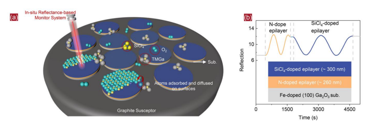
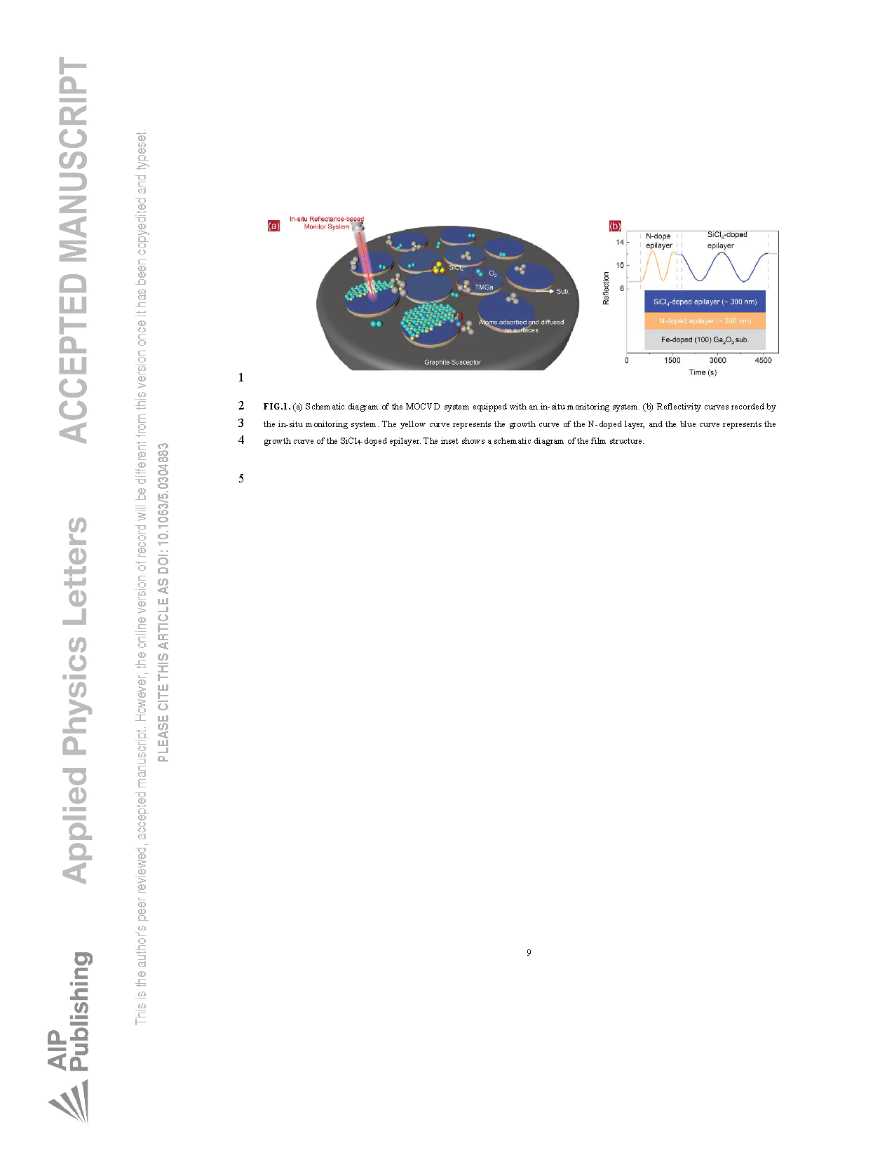
FIG. 1 (a) Schematic diagram of the MOCVD system equipped with an in-situ monitoring system. (b) Reflectivity curves recorded by the in-situ monitoring system. The yellow curve represents the growth of the N-doped layer, and the blue curve represents the growth of the SiCl₄-doped epilayer. The inset shows a schematic diagram of the film structure.

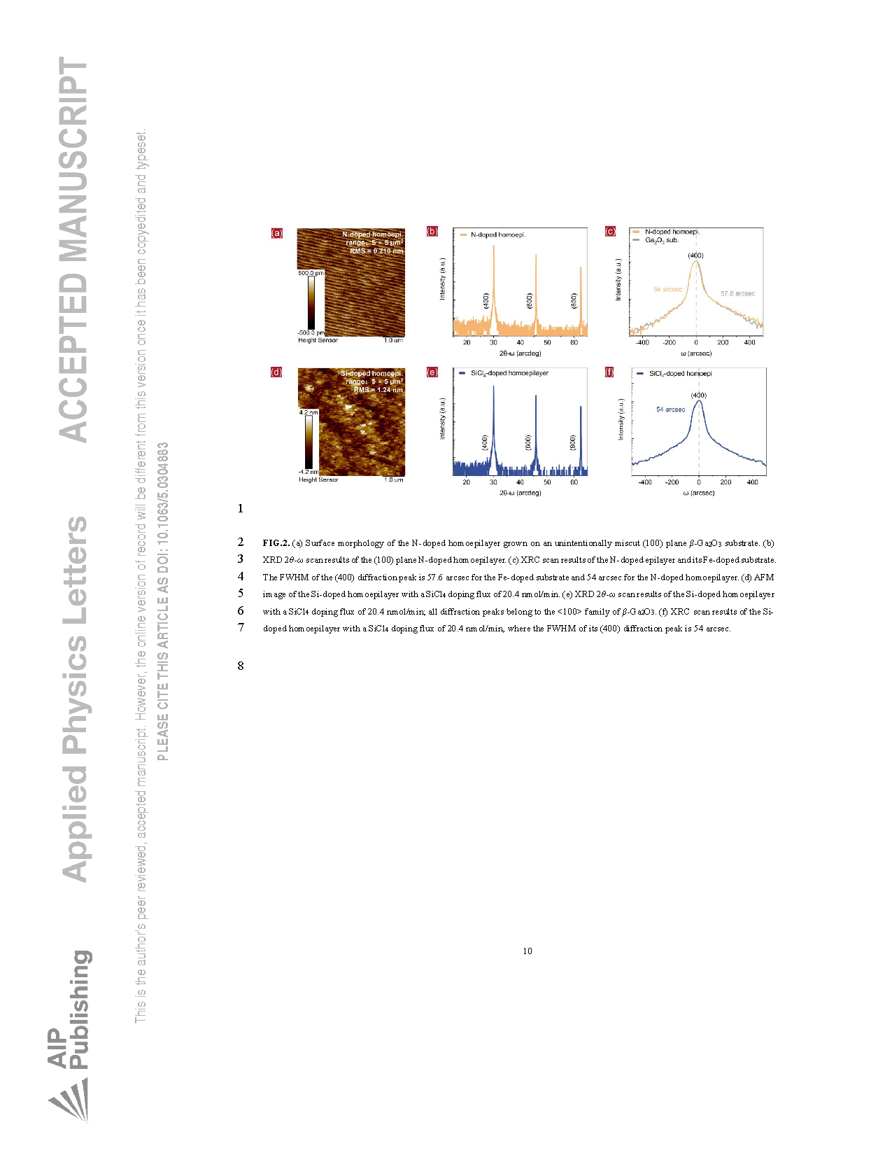
FIG. 2 (a) Surface morphology of the N-doped homoepilayer grown on an unintentionally miscut (100) plane β-Ga₂O₃ substrate. (b) XRD 2θ–ω scan results of the (100) plane N-doped homoepilayer. (c) XRC scan results of the N-doped epilayer and its Fe-doped substrate. The FWHM of the (400) diffraction peak is 57.6 arcsec for the Fe-doped substrate and 54 arcsec for the N-doped homoepilayer. (d) AFM image of the Si-doped homoepilayer with a SiCl₄ doping flux of 20.4 nmol/min. (e) XRD 2θ–ω scan results of the Si-doped homoepilayer with a SiCl₄ doping flux of 20.4 nmol/min; all diffraction peaks belong to the <100> family of β-Ga₂O₃. (f) XRC scan results of the Si-doped homoepilayer with a SiCl₄ doping flux of 20.4 nmol/min, where the FWHM of its (400) diffraction peak is 54 arcsec.

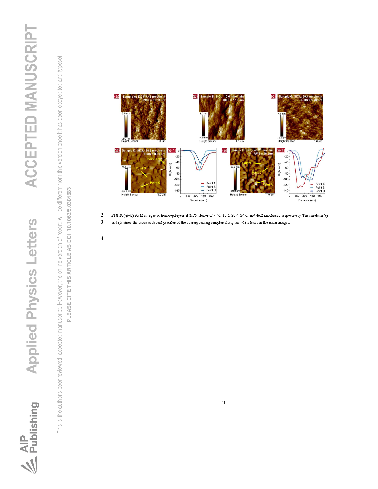
FIG. 3 (a)–(f) AFM images of Si-doped homoepilayers grown at SiCl₄ fluxes of 7.46, 10.6, 20.4, 34.6, and 46.2 nmol/min, respectively. The insets in (e) and (f) show the cross-sectional profiles of the corresponding samples along the white lines in the main images.

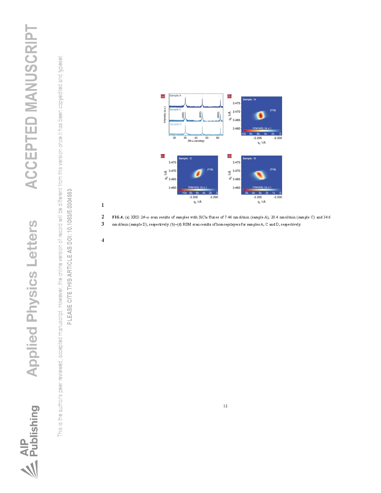
FIG. 4 (a) XRD 2θ–ω scan results of samples grown with SiCl₄ fluxes of 7.46 nmol/min (sample A), 20.4 nmol/min (sample C), and 34.6 nmol/min (sample D), respectively. (b)–(d) Reciprocal space mapping (RSM) scan results of the homoepilayers for samples A, C, and D, respectively.
DOI:
doi.org/10.1063/5.0304883