Paper Sharing
【Domestic Papers】Stable Memristive Switching Mechanism in CeO₂/a-Ga₂O₃ Heterostructure toward Synaptic Plasticity and Logical Operations
日期:2026-01-21阅读:471
Researchers from the Zhejiang Sci-Tech University have published a dissertation titled "Stable Memristive Switching Mechanism in CeO2/a-Ga2O3 Heterostructure toward Synaptic Plasticity and Logical Operations" in Materials Today Physics.
Project Support
This work was supported by the Zhejiang Provincial Natural Science Foundation of China (LQ24F040002), the National Natural Science Foundation of China (No. 62304205, 62274148, 62374147, U23A20349), the Science Foundation of Zhejiang Sci-Tech University (No. 22062337-Y, 25062169-Y), and the Funds of the Natural Science Foundation of Hangzhou (No. 2024SZRZDF040001).
Abstract
Ga2O3 has emerged as a highly promising candidate for next-generation memristive materials, owing to its ultra-wide bandgap, exceptional chemical stability, and tunable defect energy states. However, single-layer Ga2O3 memristors often suffer from unstable switching voltages caused by the random formation and rupture of conductive filaments, hindering their practical application. In this work, a CeO2/amorphous-Ga2O3 (a-Ga2O3) heterostructure memristor with a high oxygen-vacancy gradient was fabricated by employing oxygen-vacancy-rich CeO2 as an oxygen-vacancy reservoir. The conductance change arises from reversible vacancy migration rather than filament formation in this device, ensuring stable and uniform switching. The device exhibits excellent switching uniformity, with the coefficient of variation for Vset and Vreset as low as 0.18 and 0.15, respectively, which are significantly improved compared with those of the single-layer a-Ga2O3 device (0.40 and 0.53, respectively). Moreover, both the HRS and LRS states remain highly stable for up to 104 s under dark conditions. This work provides an effective approach to achieve stable, uniform, and non-filamentary resistive switching in wide-bandgap oxide memristors, paving the way for reliable neuromorphic and logic device applications.
Conclusion
In summary, this study reports a memristor based on CeO2/a-Ga2O3. Compared with the single-dielectric memristor of a-Ga2O3, this device has a more stable switching voltage in the dark state and under light, and the HRS and LRS can maintain good stability within 104 s. Meanwhile, we successfully achieved logical operations by regulating light and voltage, demonstrating the potential for application in the fields of information transmission and data security encryption. Furthermore, we conducted an in-depth study on the synaptic performance of the CeO2/a-Ga2O3 memristor. By altering different stimulation parameters, the device successfully transformed from STP to LTP and successfully simulated the process of learning-forgetting-relearning, demonstrating that this memristor has excellent neural simulation capabilities. This provides a more stable device foundation for the application of memristors in neuromorphic computing. This research can provide assistance and reference for other scholars to study the application of memristors in logical operations and neuromorphic computing, and offer more reliable and stable solution references for fields such as visual recognition and information security.
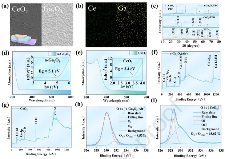
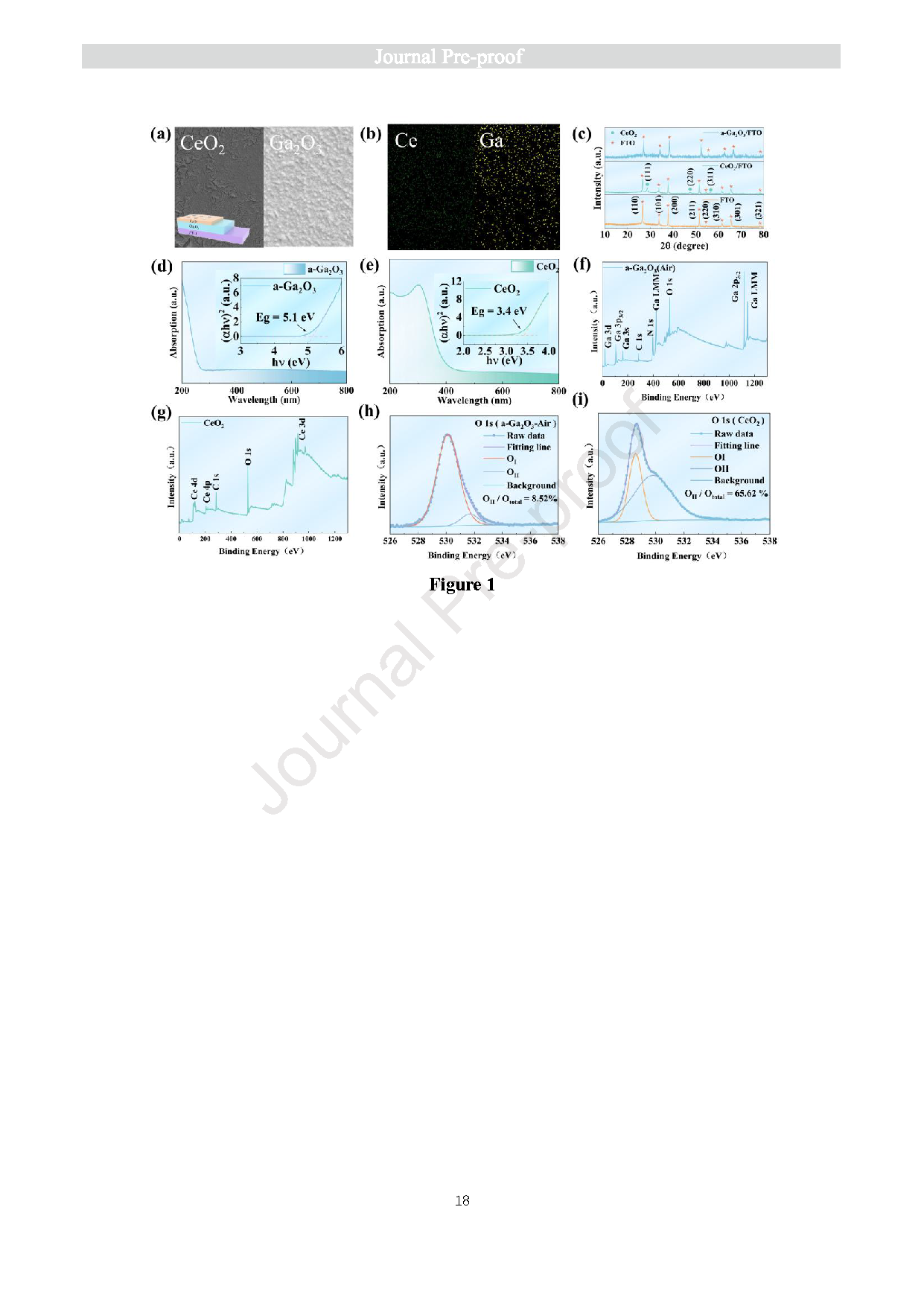
Figure 1. (a) Surface SEM image of the a-Ga2O3 film and CeO2 film. (b) The energy dispersive spectra (EDS) mapping of CeO2 and a-Ga2O3. (c) XRD patterns of a-Ga2O3/FTO, CeO2/FTO and FTO. (d) Optical absorption spectra of a-Ga2O3. (e) Optical absorption spectra of CeO2. (f) XPS spectra of a-Ga2O3. (g) XPS spectra of CeO2. (h) XPS O1s of a-Ga2O3 annealed in air. (i) XPS O1s of CeO2.
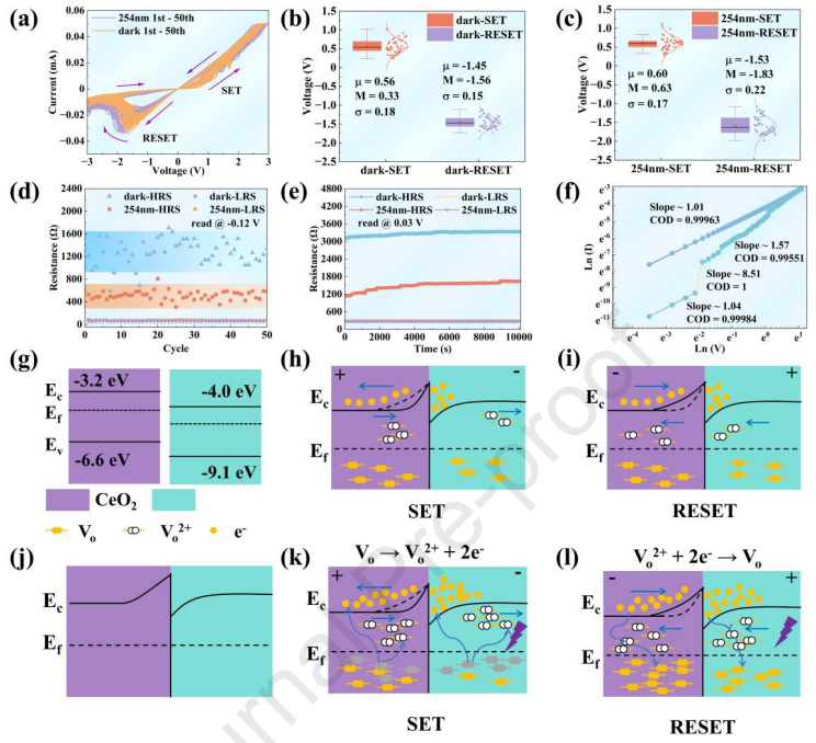
Figure 2. (a) The I-V curves of CeO2/a-Ga2O3 in the dark and under 254nm light. (b) The distribution range of VSet and VReset of CeO2/a-Ga2O3 memristors in the dark. (c) The distribution range of VSet and VReset of CeO2/a-Ga2O3 memristors under 254 nm light. (d) The trend of HRS and LRS change in the dark and 254 nm light over 50 cycles by reading at -0.12 V. (e) Retention characteristics by reading at 0.03 V. (f) The linear fitting for a Ln-Ln scale. (g) Schematic energy band diagram of CeO2 and a-Ga2O3 before contact. (h) The energy band diagram of the SET process. (i) The energy band diagram of the RESET process. (j) Schematic diagram of the energy bands of CeO2 and a-Ga2O3 after contact. (k) Band diagram of the SET process under 254nm. (l) Energy band diagram of the RESET process under 254nm.
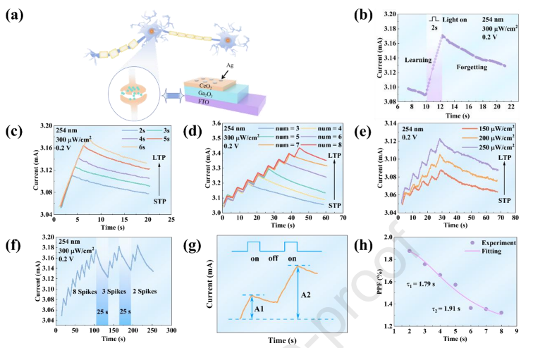
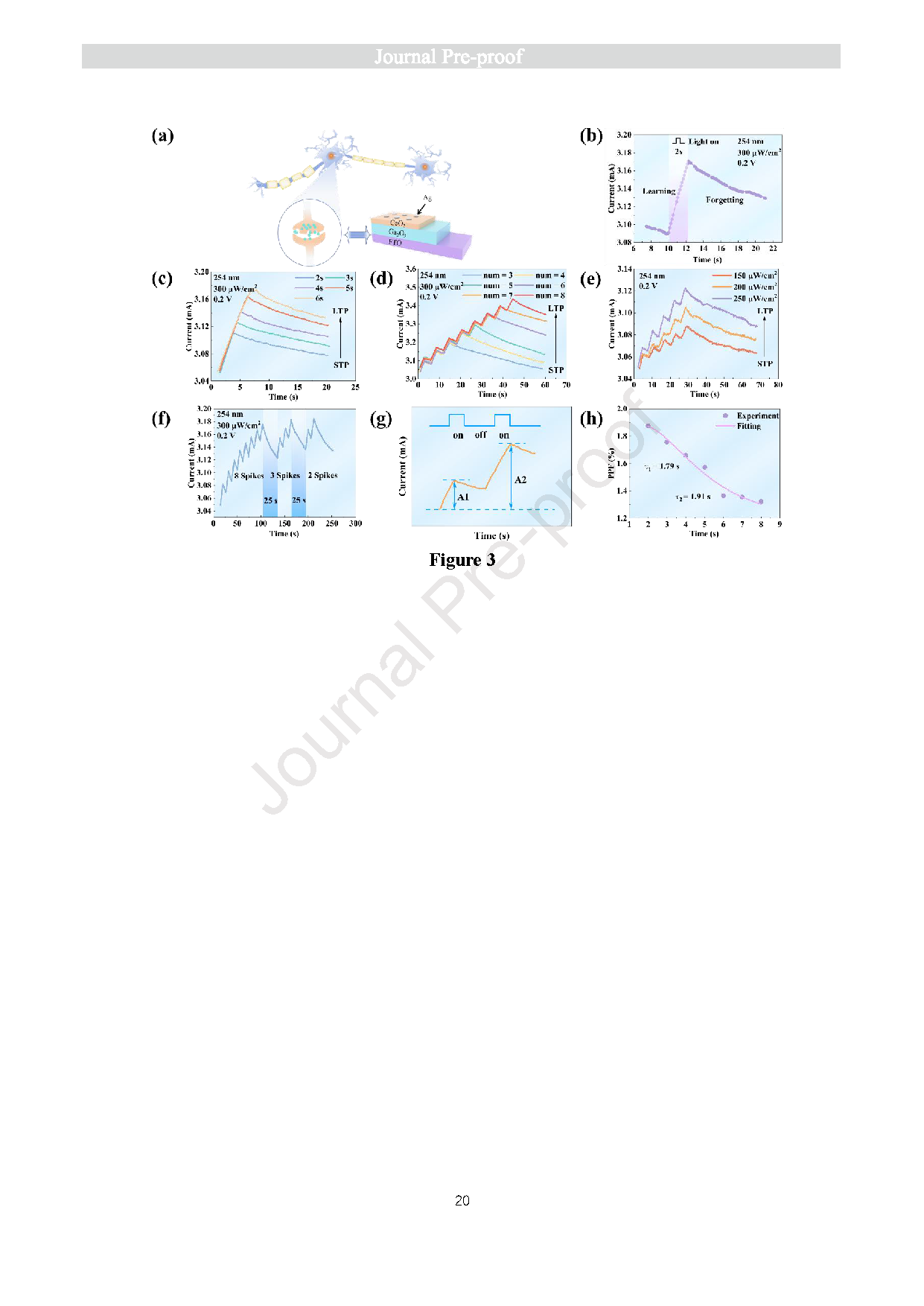
Figure 3. (a) Pictorial representations of CeO2/a-Ga2O3 devices and biological synapse. (b) EPSC triggered by a single 254 nm light pulse with a pulse width of 2 s. (c) EPSC triggered by single 254 nm light pulses with different pulse widths. (d) EPSC triggered by single 254 nm light pulses with different pulse counts. (e) EPSC triggered by different 254 nm light pulses with varying intensities. (f) Learning experience of the device. (g) The PPF of the photovoltaic synapse under a pair of light pulse stimulations. (h) The relationship between PPF index and time interval under different pulse widths.
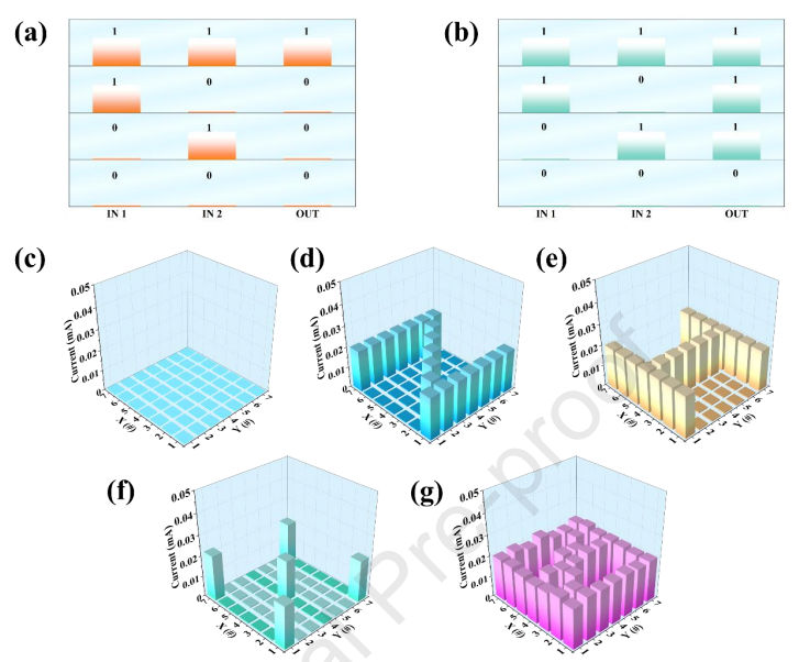
Figure 4. (a) The “AND” logic gate truth table. (b) The “OR” logic gate truth table. (c) Initial state of the device. (d) The state of the device under the application of an electrical pulse. (e) The state of the device under the application of light pulses. (f) Output the result of “AND Gate”. (g) Output the result of “OR Gate”.
DOI:
doi.org/10.1016/j.mtphys.2026.102014