Paper Sharing
【Domestic Papers】Gallium-Based Semiconductor Integrated Circuits: Past, Present, and Future for Emerging Optoelectronic Devices
日期:2026-01-26阅读:429
Researchers from the Fuzhou University have published a dissertation titled "Gallium-Based Semiconductor Integrated Circuits: Past, Present, and Future for Emerging Optoelectronic Devices" in Advanced Functional Materials.
Background
For decades, Si has dominated the landscape of electronic devices, underpinning power electronics, optoelectronics and photovoltaics. Today, an estimated 87% of the global electronics market is still built on Si-based technologies. However, a persistent paradox remains: the maturity of Si technology is increasingly at odds with the intrinsic physical limitations of the material. This tension has become more pronounced with the growing demand for high-performance and diversified applications. In parallel, rapid advances in emerging sectors-ranging from 5G/6G communications and megawatt fast charging to electric vehicle power systems, solid-state lighting, high-voltage electronics and deep-ultraviolet detection have propelled Gabased semiconductors (GaAs, GaN, Ga2O3, and GaSb) to the forefront of research and industry. Their unique properties have positioned them as key candidates to extend performance beyond the Si family, enabling transformative applications across power electronics and optoelectronics.
Abstract
As the cornerstone of modern electronic technology, Ga-based semiconductors encompassing GaN, GaAs, Ga2O3, and GaSb have emerged as core materials for next-generation optoelectronic applications, spanning consumer electronics, power devices, optical communication systems, and quantum technologies. This review systematically assesses their intrinsic properties, such as wide bandgaps, high electron mobility, and excellent thermal stability, which underpin technological breakthroughs in micro-LEDs, power electronics, photodetectors, photonics, and sensing technologies. By examining advances in scalable fabrication technologies and innovative device architectures, this study emphasizes their transformative potential in frontier fields including AR, high-speed communication, and energy-efficient electronics. Collectively, this review highlights the pivotal role of Ga-based semiconductors in propelling the development of next-generation electronics and photonics, while elaborating on current challenges and outlining promising directions for future research.
Conclusions
Ga-based semiconductors have exhibited transformative potential across electronic and optoelectronic applications, owing to their unique intrinsic properties, including wide bandgaps, high electron mobility, and excellent thermal stability. In power electronics, GaN HEMTs achieve VB exceeding 1.1 kV, benefiting from high electron mobility (2000 cm2⋅V−1 ⋅s−1) and 2DEG, while p-GaN gate structures enable reliable normally-off operation. β-Ga2O3 Schottky barrier diodes have set a record VB of 8.32 kV with a PFOM of 13.21 GW⋅cm−2, surpassing the theoretical limits of SiC and GaN. For optoelectronic applications, GaNbased Micro-LEDs attain a luminous efficacy of 307 lm⋅W−1 and a visible light communication rate of 7.48 Gb⋅s−1, where nanowire structures effectively mitigate the quantum-confined Stark effect. GaAs quantum dots enable high-efficiency single-photon emission through bandgap engineering, while GaSb/InAs typeII superlattices realize tunable infrared detection (3–32 µm) with high detectivity (1.7 × 1011 cm⋅Hz0.5⋅W−1 at 80 K).
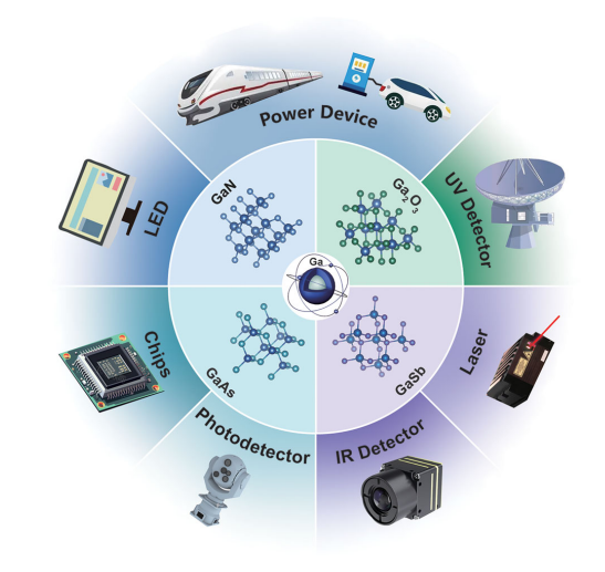
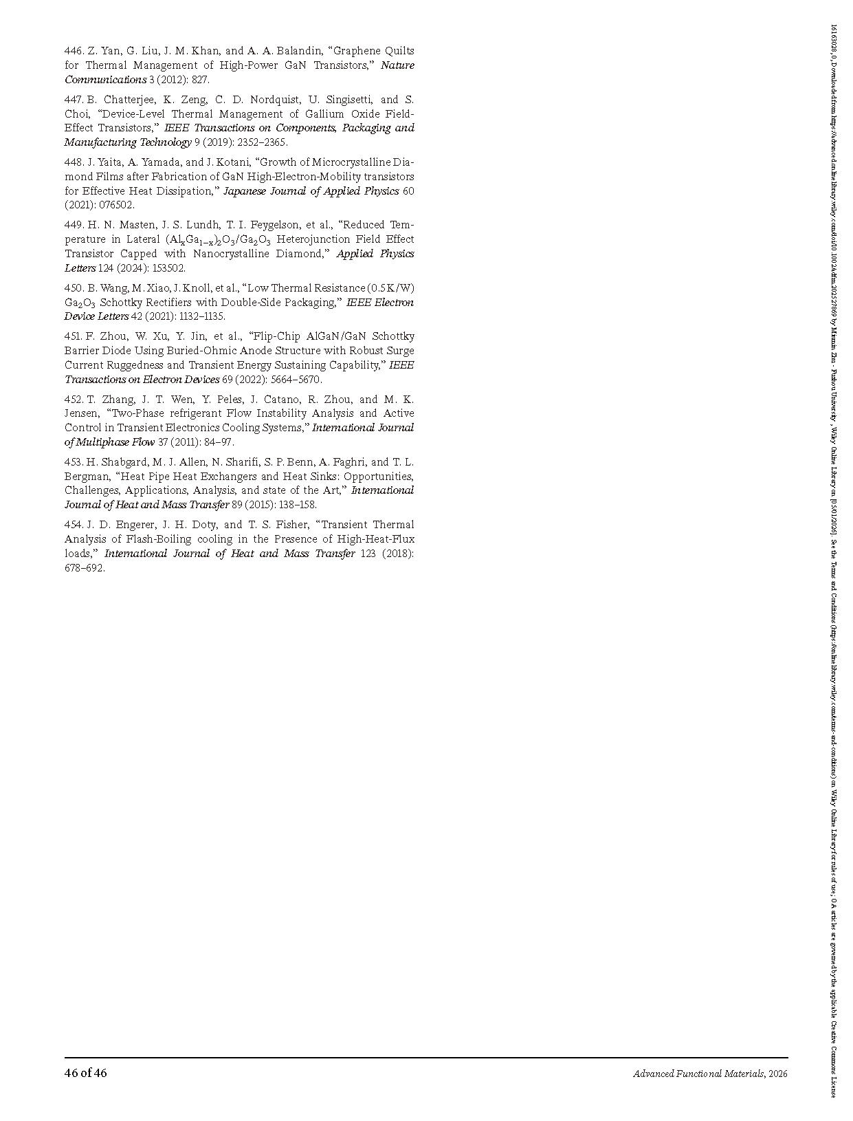
FIGURE 1 Major application areas of Ga family members.
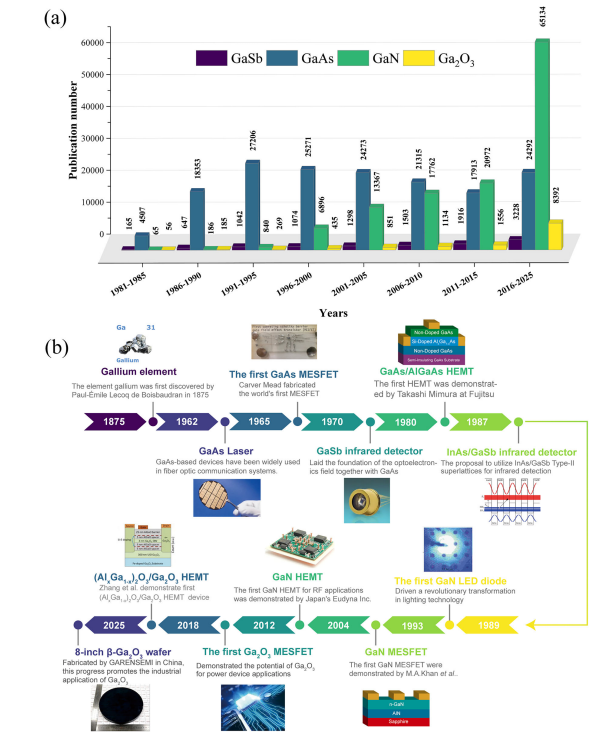
FIGURE 2 (a) Number of publications on GaN, GaAs, GaSb, and Ga2O3 over recent decades (data from Web of Science with the key words of “GaN,” “GaAs,” “GaSb,” and “Ga2O3”; the search date is 1 November 2025). (b) Timeline for the development of the Ga family. Inset images: “(AlxGa1−x)2O3/Ga2O3 HEMT” reproduced with permission, Copyright 2018, AIP Publishing LLC. “InAs/GaSb infrared detector.” Reproduced under terms of the CC-BY license. Copyright 2014, Author(s), published by Wiley-VCH.
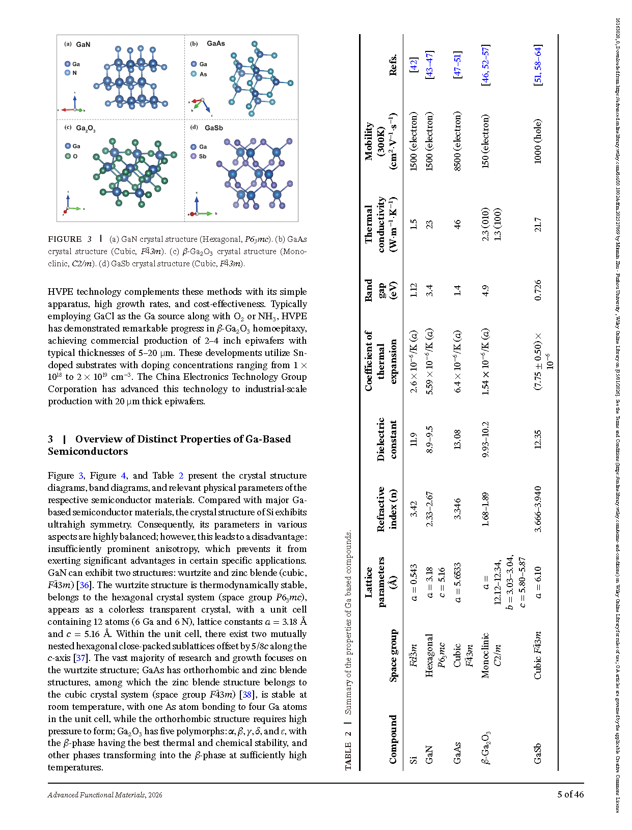
FIGURE 3 (a) GaN crystal structure (Hexagonal, P63mc). (b) GaAs crystal structure (Cubic, F-43m). (c) β-Ga2O3 crystal structure (Monoclinic, C2/m). (d) GaSb crystal structure (Cubic, F-43m).
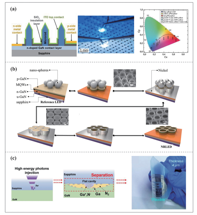
FIGURE 4 The band structures of (a) GaN. Reproduced with permission. Copyright 1971, Elsevier. The band structures of (b) GaAs. Reproduced with permission. Copyright 2004, American Physical Society. (c) The band structures of β-Ga2O3. Reproduced with permission. Copyright 2015, Wiley-VCH. (d) The band structures of GaSb. Reproduced with permission. Copyright 1969, American Physical Society.
DOI:
doi.org/10.1002/adfm.202527869