Paper Sharing
【International Papers】Mist-chemical vapor deposition grown Ge-doped α-Ga₂O₃ thin films with high electron mobility
日期:2026-01-26阅读:381
Researchers from the Kyoto University have published a dissertation titled "Mist-chemical vapor deposition grown Ge-doped α-Ga2O3 thin films with high electron mobility" in Applied Physics Letters.
Background
Ga2O3 is a promising material for power electronics, high-frequency devices, and ultraviolet detectors because of its large bandgap (~5 eV). Thin-film growth, fundamental electrical properties, and applications of β-Ga2O3—the most thermodynamically stable Ga2O3 phase—have been actively investigated. Another polymorph of Ga2O3, α-Ga2O3, has attracted considerable attention because of its wide bandgap (5.3–5.6 eV) and high estimated breakdown field (9.5 MV/cm), which exceed those of β-Ga2O3 (4.5–4.8 eV and 6.5 MV/cm, respectively). Although the metastable α-Ga2O3 phase generally tends to transform into thermodynamically stable β-Ga2O3 at 600–700 °C, the use of an AlOx capping layer or selective area growth can raise the temperature of this transition to 800–900 °C.
Abstract
Unintentionally doped and Ge-doped α-Ga2O3 films were grown on m-plane sapphire substrates via mist-chemical vapor deposition at a substrate temperature of 600 °C and a growth rate of 3.3 μm/h. Hall-effect measurements at room temperature indicated that the unintentionally doped film exhibited a low carrier concentration of 3 × 1016 cm−3, and the highest electron mobility reached 99 cm2 V−1 s−1 for the Ge-doped α-Ga2O3 film with a carrier concentration of 5.8 × 1017 cm−3. Temperature-dependent Hall-effect measurements clarified the transport mechanism: scattering caused by dislocations and ionized impurities dominate at low temperatures in films with carrier concentrations of 1.7 × 10¹⁷ and 5.8 × 1017 cm−3, respectively, whereas polar optical phonons are the main origin of electron scattering around room temperature. The average densities of threading screw and edge dislocations in Ge-doped films prepared herein are 6.0 × 10⁸ and 1.1 × 109 cm−2, respectively, which are lower than those for α-Ga2O3 films grown on sapphire substrates to date. The low carrier concentration and high electron mobility achieved by reducing the dislocation density suggest the promising application potential of α-Ga2O3 in power electronics and high-frequency devices.
Conclusion
In conclusion, UID and Ge-doped α-Ga2O3 films were grown on m-plane sapphire substrates using mist-CVD at the growth temperature of 600 °C and growth rate of 3.3 lm/h. A low carrier concentration (3 × 1016 cm-3) was achieved for the UID α-Ga2O3 film. The highest electron mobility reached 99 cm2 V-1 s-1 at a carrier concentration of 5.8 × 1017 cm-3. The room-temperature mobilities of the present α-Ga2O3 films with carrier concentrations higher than 1017 cm-3 are comparable to the mobilities of β-Ga2O3 with similar carrier concentrations. The results of temperature-dependent Hall-effect measurements showed that the dominant scattering factor changes from dislocation scattering to ionized impurity scattering with increasing carrier concentration. The densities of threading edge and screw dislocations in the present α-Ga2O3 films were estimated from XRD rocking curves as 6.0 × 10⁸ and 1.1 × 109 cm-2, respectively. These values are comparable to those for α-Ga2O3 films with buffer layers. The lower dislocation density leads to higher mobility at low carrier concentrations, as described above. These results prove the promising potential of α-Ga2O3 for applications in high-voltage and high-frequency power electronics devices.
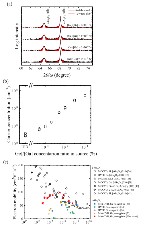
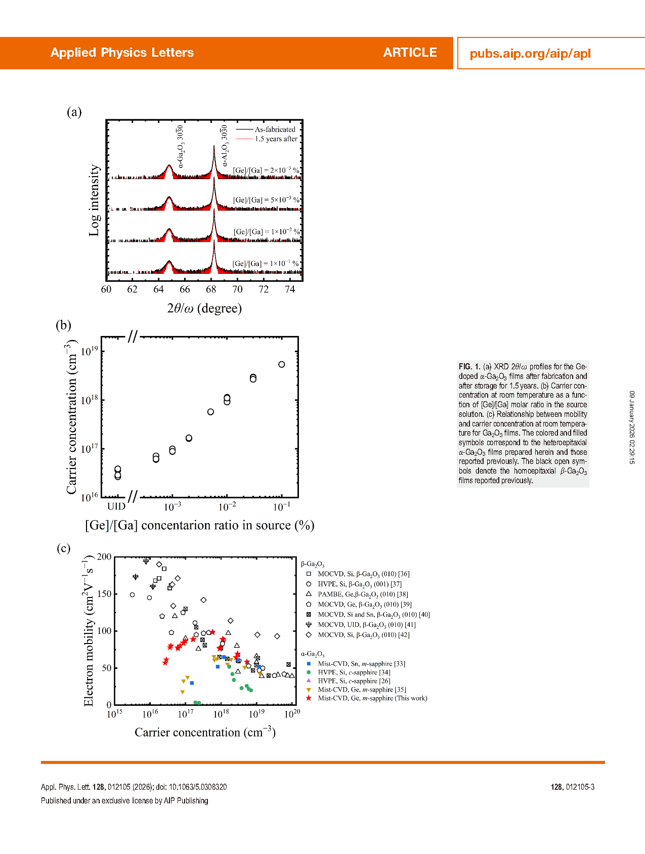
FIG. 1. (a) XRD 2θ/x profiles for the Ge-doped a-Ga2O3 films after fabrication and after storage for 1.5 years. (b) Carrier concentration at room temperature as a function of [Ge]/[Ga] molar ratio in the source solution. (c) Relationship between mobility and carrier concentration at room temperature for Ga2O3 films. The colored and filled symbols correspond to the heteroepitaxial α-Ga2O3 films prepared herein and those reported previously. The black open symbols denote the homoepitaxial β-Ga2O3 films reported previously
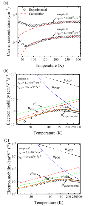
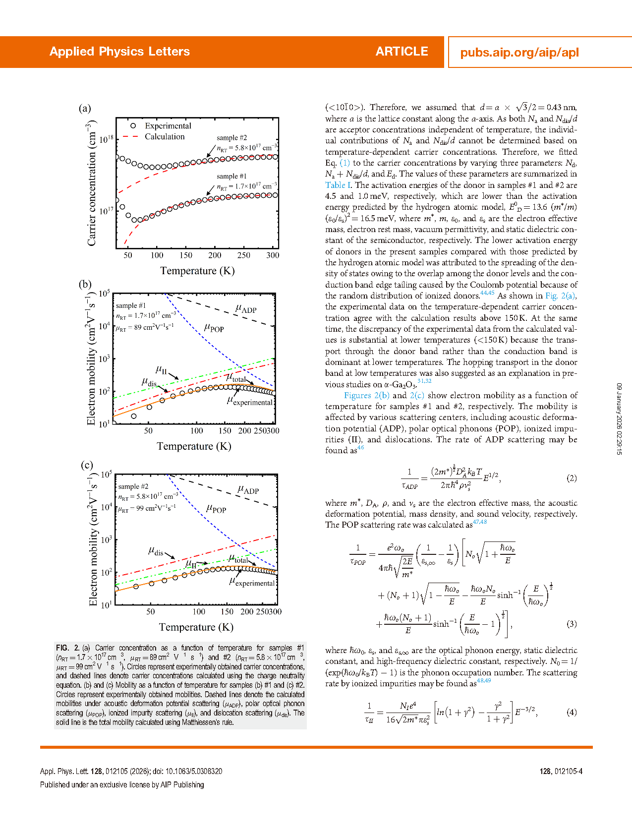
FIG. 2. (a) Carrier concentration as a function of temperature for samples #1 (nRT = 1.7 × 1017 cm-3 , lRT = 89 cm2 V-1 s-1) and #2 (nRT = 5.8 × 1017 cm-3 , lRT = 99 cm2 V-1 s-1). Circles represent experimentally obtained carrier concentrations, and dashed lines denote carrier concentrations calculated using the charge neutrality equation. (b) and (c) Mobility as a function of temperature for samples (b) #1 and (c) #2. Circles represent experimentally obtained mobilities. Dashed lines denote the calculated mobilities under acoustic deformation potential scattering (μADP), polar optical phonon scattering (μPOP), ionized impurity scattering (μII), and dislocation scattering (μdis). The solid line is the total mobility calculated using Matthiessen’s rule.
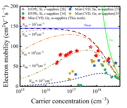
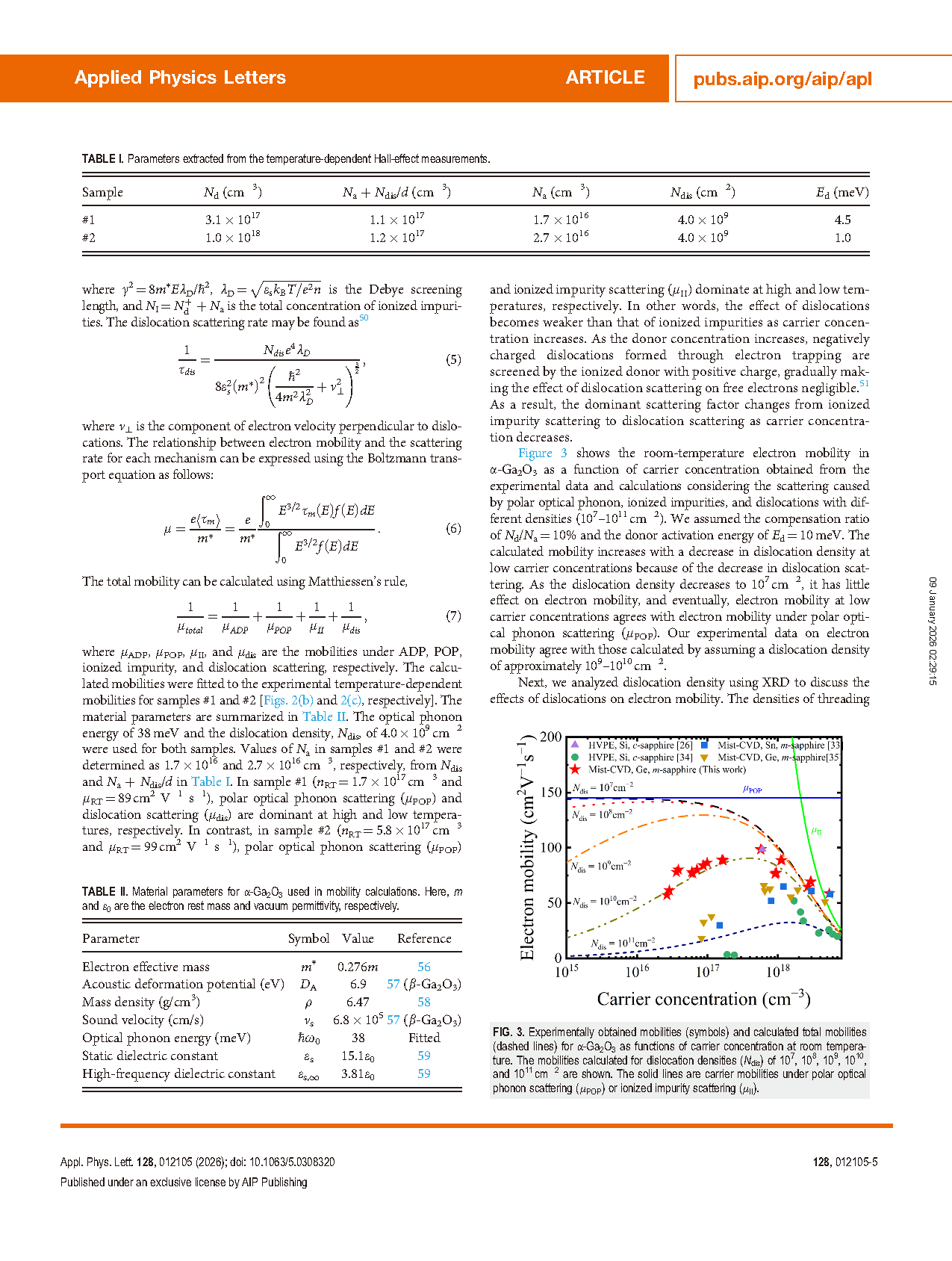
FIG. 3. Experimentally obtained mobilities (symbols) and calculated total mobilities (dashed lines) for α-Ga2O3 as functions of carrier concentration at room temperature. The mobilities calculated for dislocation densities (Ndis) of 107, 108, 109, 1010, and 1011 cm-2 are shown. The solid lines are carrier mobilities under polar optical phonon scattering (μPOP) or ionized impurity scattering (μII).
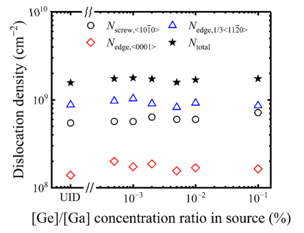
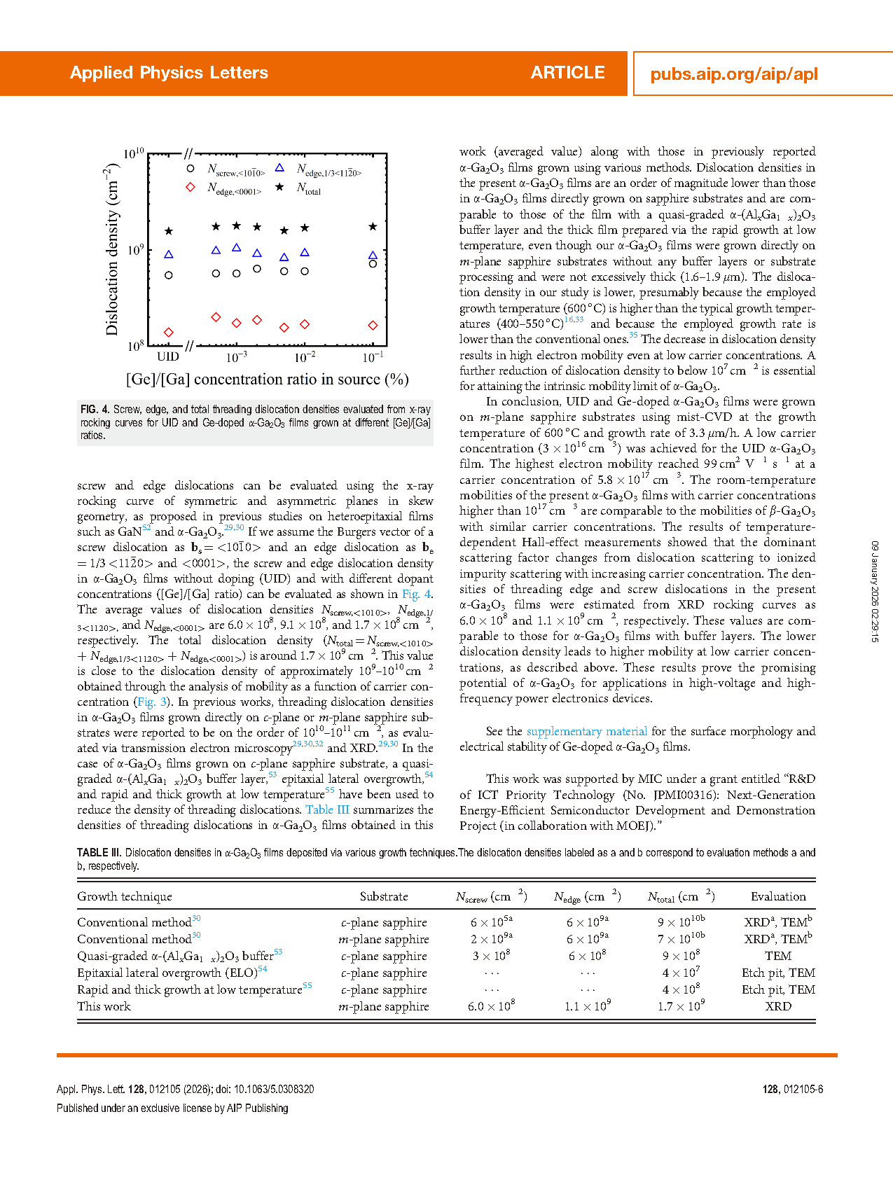
FIG. 4. Screw, edge, and total threading dislocation densities evaluated from x-ray rocking curves for UID and Ge-doped α-Ga2O3 films grown at different [Ge]/[Ga] ratios.
DOI:
doi.org/10.1063/5.0308320