


Alliance News
【Alliance News】Multiple Breakthroughs Across the Global Gallium Oxide Industry in 2025
日期:2026-01-26阅读:2341
Introduction
In 2025, the global gallium oxide industry continued to evolve steadily. International companies made a series of new moves in capacity expansion, partnership development, and market deployment, further advancing the maturation of the industrial ecosystem. Based on publicly available information continuously tracked and released by the Alliance platform, it can be observed that enterprises from Japan, Germany, the United Kingdom, the United States, South Korea, and other countries are progressing at different paces across various segments of the value chain, collectively driving the steady improvement of the industry landscape.
The following overview takes readers to the forefront of the international gallium oxide industry, highlighting corporate strategies, collaborative practices, and market activities within a global context, and offering a comprehensive view of the vitality and development momentum of the worldwide industry.
Novel Crystal Technology: Continuing to Lead the Global Gallium Oxide Industry
In 2025, Novel Crystal Technology, Inc. (NCT) of Japan, a global leader in the Gallium Oxide industry, achieved a series of major breakthroughs throughout the year.
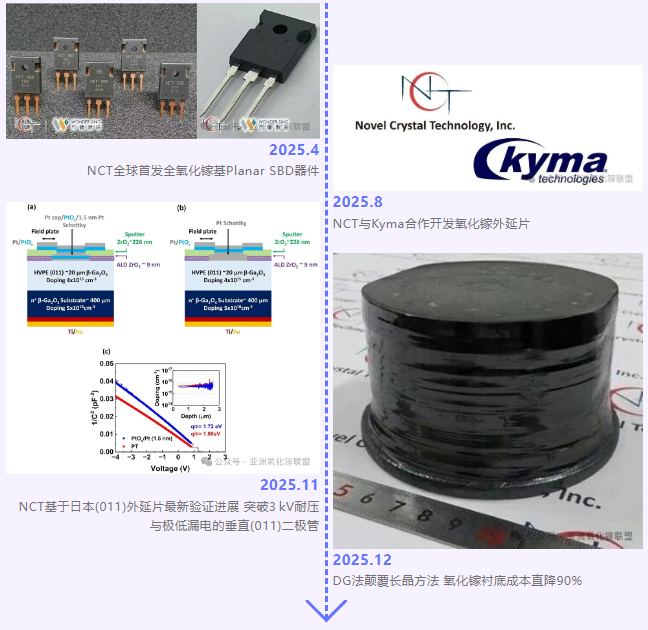
In April, NCT globally launched the first all–Gallium Oxide–based planar Schottky barrier diode (Planar SBD) devices. Research Sample (RS)–grade products were made available for scientific research and early-stage application exploration. Two electrode configurations were offered to meet different testing requirements, providing valuable verification and analysis opportunities for industry users.
In August, NCT partnered with Kyma Technologies (USA) to jointly develop high-quality Ga₂O₃ epitaxial wafers targeting the commercialization of multi-kV power devices. By combining NCT’s substrate manufacturing strengths with Kyma’s epitaxial growth expertise, the collaboration accelerated the industrialization of large-area, low-defect-density epitaxial wafers, providing critical support for high-voltage power electronics markets such as electric vehicles, renewable energy, and aerospace.
In November, NCT introduced its (011)-oriented series of high-quality epitaxial wafers. The epitaxial thickness was increased from 20 μm to 30 μm, carrier concentration was precisely controlled at 2–5 × 10¹⁵ cm⁻³, and defect density was reduced to 5 pcs/cm², reaching industry-leading levels and providing strong technical assurance for performance breakthroughs in high-end power devices.
In December, under a project supported by NEDO, NCT successfully developed the Drop-fed Growth (DG) method. This technique eliminates the need for expensive iridium crucibles by supplying the melt material in droplet form, reducing the manufacturing cost of β-Ga₂O₃ substrates to one-tenth of conventional methods. This breakthrough laid a solid foundation for low-cost substrate production and large-scale industrialization.
Overall, NCT’s continuous advancements across device development, epitaxial wafer production, and crystal growth technologies throughout 2025 not only reinforced its position as an international industry leader, but also injected new momentum into the steady development of the global Gallium Oxide industry.
FLOSFIA: From Key Device Breakthroughs to Mass-Production Validation
In the field of Gallium Oxide power semiconductors, FLOSFIA—a Japanese company focused on α-Ga₂O₃—has shown a clearly phased progression in its developments over the past year.
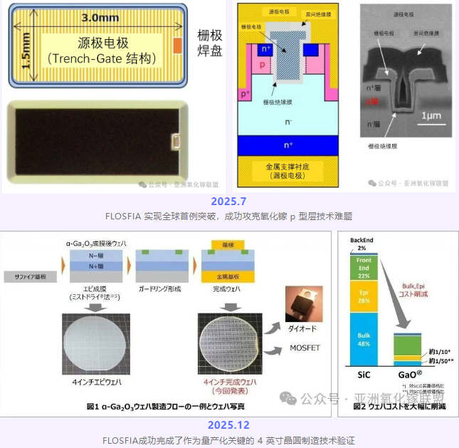
In mid-2025, FLOSFIA was the first to realize normally-off operation in α-Ga₂O₃ MOSFETs based on a p-type layer structure, and successfully validated device performance under relatively high current conditions. This achievement broke through a core structural challenge long regarded as a major barrier to the practical application of Gallium Oxide devices, demonstrating the engineering feasibility of a complete device architecture.
Subsequently, toward the end of 2025, FLOSFIA further advanced its R&D focus toward mass-production readiness. The company completed manufacturing technology validation on 4-inch wafers and, in parallel, resolved key issues related to reliability and uniformity in diode devices, laying the groundwork for stable volume production of future product lines.
Overall, FLOSFIA is transitioning from isolated device-level breakthroughs to a more systematic development stage centered on manufacturing feasibility and mass-production stability, with an increasingly clear and well-defined technology roadmap.
Japan Mitsubishi Electric: Disclosure of Gallium Oxide–Related R&D Activities
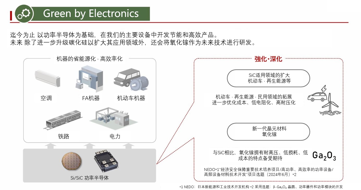
In March 2025, Mitsubishi Electric—one of the world’s leading suppliers of advanced electronic equipment and systems—showcased its cutting-edge technological achievements at its Advanced Technology R&D Center and announced that it would pursue research and development on Gallium Oxide (Ga₂O₃) materials. This Gallium Oxide technology has already been adopted since June 2024 under the New Energy and Industrial Technology Development Organization (NEDO) program titled “Economic Security–Focused Key Technology Development Project / Materials Technology Development for High-Power, High-Efficiency Power Devices and High-Frequency Devices”, and is being advanced with NEDO’s support.
This move indicates that Mitsubishi Electric is actively positioning itself in the Gallium Oxide field, underscoring the strategic importance of Gallium Oxide in the next generation of wide-bandgap semiconductor technologies.
Swansea University CISM: Establishing the First Platform for 4-Inch Gallium Oxide Thin-Film Growth
In April 2025, the Centre for Integrated Semiconductor Materials (CISM) at Swansea University in South Wales, UK, established the country’s first platform capable of growing high-quality Gallium Oxide thin films on 4-inch substrates. The platform is based on a newly commissioned AIXTRON Close Coupled Showerhead (CCS) deposition system and was funded by a £2.7 million strategic equipment grant from the UK Engineering and Physical Sciences Research Council (EPSRC). The system is installed in a newly built Oxide and Chalcogenide MOCVD laboratory, which has now become a national-level R&D hub for Gallium Oxide thin-film research in the UK. Research activities span power electronics, deep-ultraviolet photodetectors, and transparent conductive oxide (TCO) applications.
In June 2025, CISM also signed an agreement with UK microgravity manufacturing company Space Forge, becoming the first industrial tenant of the center. Through this collaboration, Space Forge gains access to the full suite of semiconductor processing and characterization facilities to conduct manufacturing research under microgravity conditions.
With both the equipment platform and collaborative research initiatives now in place, Gallium Oxide is receiving increasing attention within the UK power electronics research ecosystem, and its potential for high-performance power device applications is being further evaluated.
IKZ: Gallium Oxide Semiconductor Materials Technology Development Project Officially Launched
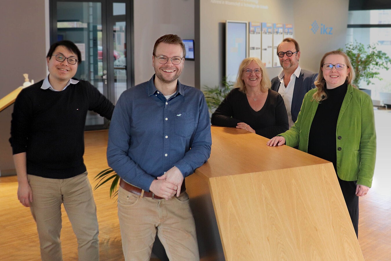
In April 2025, Germany’s Leibniz Institute for Crystal Growth (IKZ), a research institution specializing in crystal growth and materials development, released the latest progress of the EFRE project “G.O.A.L. – Gallium Oxide Application Laboratory for Power Electronics.” Although the project was initiated in September 2024, its practical significance within the Gallium Oxide technology landscape has become increasingly clear as key equipment and technical capabilities were fully deployed in 2025.
Globally, Japan, South Korea, and China have successively advanced government-led Gallium Oxide–related programs, while in the United States the field has been continuously driven primarily by the Air Force system. Against this backdrop, Europe—and Germany in particular—is accelerating a more systematic deployment in Gallium Oxide power electronics. Focusing on the critical conditions required to transition Gallium Oxide materials from research to device applications, the project centers on establishing a 2-inch wafer-based layer structure system, introducing industrial-grade epitaxy equipment from AIXTRON, and collaborating with other technical partners to jointly promote the engineering development of 2-inch Gallium Oxide epitaxial technologies.
Looking ahead, IKZ plans to establish itself across the European Union as a key research partner for Gallium Oxide epitaxial wafers and as a material supply node. Together with research institutions and enterprises in the Berlin–Brandenburg region, IKZ will continue to advance the development of larger-size materials and devices. As the GOAL project progresses, the material foundation for Gallium Oxide within Europe’s power electronics ecosystem is steadily taking shape, and its industrial value as a next-generation high-efficiency power semiconductor material is becoming increasingly evident.
NextGO Epi: Officially Established to Advance Innovation in Fourth-Generation Ultra-Wide-Bandgap Semiconductors
In May 2025, NextGO Epi, a company incubated by Germany’s Leibniz Institute for Crystal Growth (IKZ), officially announced its establishment in Berlin. As a manufacturer focused on the large-scale production of high-quality β-Ga₂O₃ (Gallium Oxide) epitaxial wafers, the company aims to provide critical materials for high-power electronics and optoelectronic detection applications.
NextGO Epi adopts metal-organic vapor phase epitaxy (MOVPE) technology and is committed to delivering Gallium-Oxide-based epitaxial wafers with significant cost and performance advantages for key sectors such as electric vehicles, rail transportation systems, and renewable energy infrastructure.
Overall, NextGO Epi’s deployment is not a single, isolated technological breakthrough. Instead, it represents a systematic effort centered on Gallium Oxide epitaxy, a critical link in the industrial chain, to close the capability gap between materials and device realization. This progress provides a practical materials-side anchor for Gallium Oxide to enter next-generation power electronic applications, while further confirming its clear positioning and mid- to long-term development potential within the emerging wide-bandgap semiconductor landscape.
Gallox: The World’s First Company to Commercialize Gallium Oxide Devices Selected for Activate Fellowship 2025
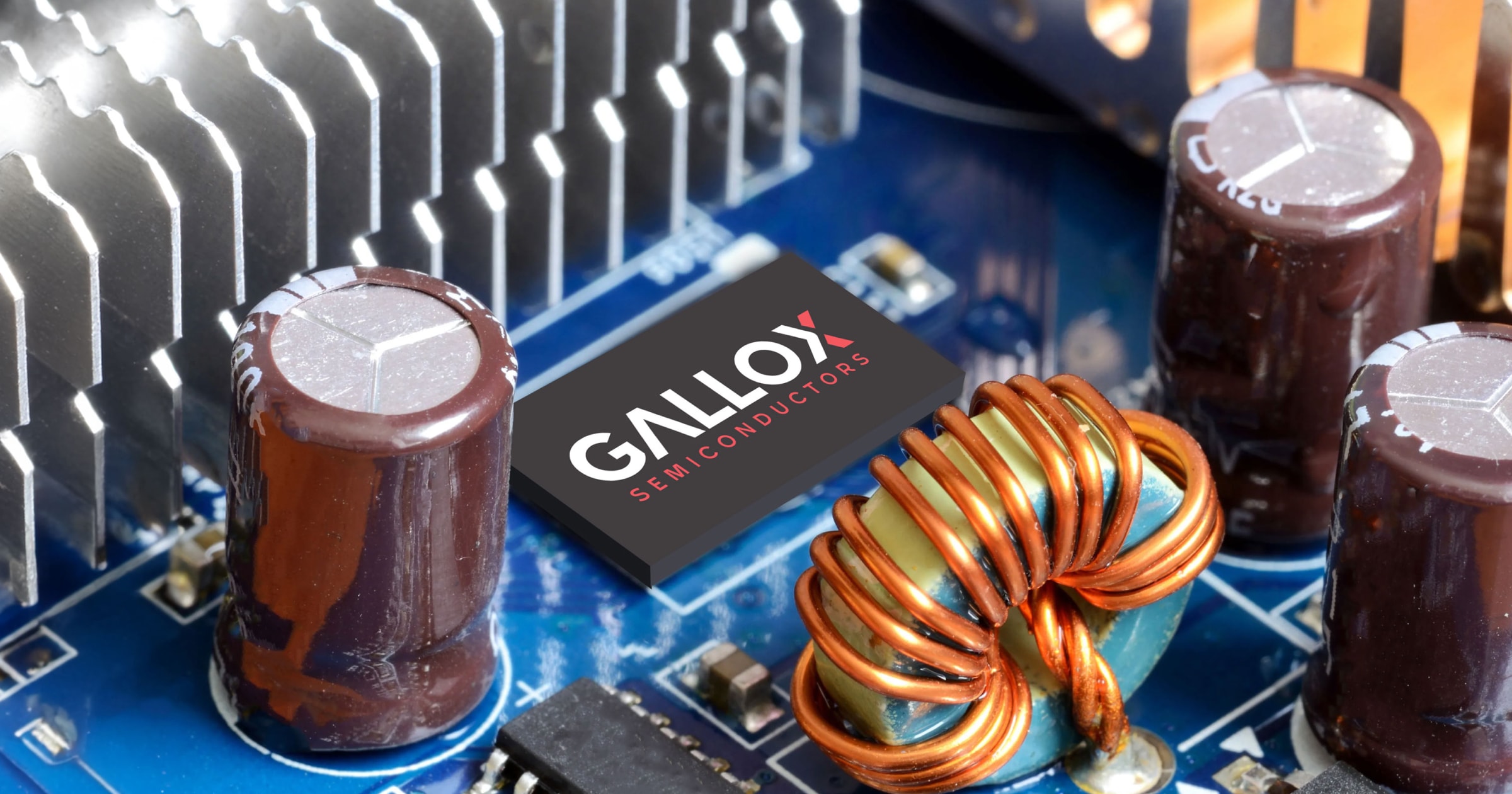
In August 2025, Gallox, a Cornell University spin-out and the world’s first company to commercialize Gallium Oxide (Ga₂O₃) devices, was selected for the Activate Fellowship 2025 program. The two-year fellowship is designed to support scientists and engineers in translating research outcomes into sustainable startup companies.
Gallox was founded by McCandless, who conducted long-term research on Gallium Oxide semiconductors during his doctoral studies at Cornell University. Compared with conventional semiconductor materials, Gallium Oxide offers lower energy consumption and higher performance potential in power devices, targeting high-power application scenarios such as data centers, drones and aerospace systems, space technologies, and electric vehicle charging.
Gallox’s selection reflects the fact that Gallium Oxide devices are increasingly entering the engineering and commercialization stage in next-generation power electronics. It also highlights how hard-tech entrepreneurship rooted in academic research is becoming an important pathway for the real-world deployment of advanced semiconductor materials.
PowerCubeSemi: The World’s First Gallium Oxide Semiconductor Manufacturer Plans IPO
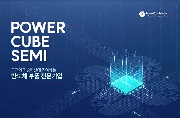
In December 2025, PowerCubeSemi, a Gallium Oxide semiconductor company, is advancing its plans for an initial public offering. The company has completed KRW 6 billion in pre-IPO financing and plans to apply for listing on KOSDAQ, South Korea’s technology-focused stock market, in 2026.
PowerCubeSemi operates the world’s first large-scale mass-production wafer fab dedicated to Gallium Oxide, and has already engaged with multiple international customers seeking high-efficiency power and RF solutions. Compared with conventional silicon materials, Gallium Oxide offers significant advantages in breakdown voltage and energy efficiency, and is gradually entering high-power application domains such as electric vehicles, data centers, and defense electronics.
Against the backdrop of South Korea incorporating next-generation semiconductor materials into its national R&D and industrial investment priorities, PowerCubeSemi’s IPO preparation is not merely an isolated corporate action. Rather, it reflects Gallium Oxide’s transition from technology validation toward an industrial stage that can be valued and supported by capital markets, providing a tangible pathway for post-silicon material strategies.
Conclusion
Ongoing initiatives from universities, research institutions, startups, and industrial capital are collectively shaping the global development landscape of Gallium Oxide. From the establishment of crystal growth and epitaxy capabilities, to device exploration and the gradual expansion of application scenarios, and further to industrialization pathways and capital deployment, Gallium Oxide has been incorporated into national strategies for next-generation power electronics and wide-bandgap materials across multiple countries.
While progress remains at different stages, the overall trajectory is becoming increasingly clear: Gallium Oxide is no longer merely a “promising material” confined to laboratories. It is now being deployed worldwide for engineering validation and entering a phase of long-term investment and continuous optimization. With sustained advancement and multi-stakeholder engagement, the pace of Gallium Oxide development is accelerating, its potential within the wide-bandgap materials ecosystem continues to unfold, and its long-term prospects are well worth anticipating.
