Paper Sharing
【Member Papers】The Demonstration of Amperometric Ga₂O₃ Two-step Trench Schottky Barrier Diode
日期:2026-01-27阅读:367
Researchers from the Jiufengshan Laboratory have published a dissertation titled "The Demonstration of Amperometric Ga2O3 Two-step Trench Schottky Barrier Diode" in 2025 22nd China International Forum on Solid State Lighting & 2025 11th International Forum on Wide Bandgap Semiconductors (SSLCHINA: IFWS).
Background
Gallium oxide (Ga₂O₃), as an emerging ultra-wide bandgap (UWBG) semiconductor material, has demonstrated significant potential for power devices due to its wide bandgap (4.8 eV), high theoretical breakdown electric field (8 MV/cm), and the ability to grow large-size crystals through the liquid-phase melt method. Schottky barrier diodes (SBDs) play a crucial role in switching power supplies, rectifier circuits, and high-frequency communication equipment, thanks to their unique metal-semiconductor junction structure. However, in conventional SBDs, the maximum electric field occurs at the metal-semiconductor interface, and the resulting image-force effect lowers the Schottky barrier height, leading to increased reverse leakage current and premature breakdown under high electric fields.
To address this issue, various methods have been proposed, including using alloys with higher Schottky barriers, high-k dielectrics, junction barrier-controlled Schottky structures, and three-dimensional “trench” device geometries. For Ga₂O₃, due to the lack of effective p-type doping, trench structures have emerged as a feasible reduced surface field (RESURF) technology. By pushing the peak electric field away from the metal-semiconductor interface into the deeper drift region, trench SBDs can effectively improve the breakdown voltage and leakage current characteristics of the device. However, trench SBDs still face challenges with electric field concentration at the trench corners, which may lead to localized breakdown and limit the potential of Ga₂O₃ in high-voltage applications.
To overcome this, multi-step trench structures have been proposed as an effective solution. Compared to single-step trenches, multi-step configurations redistribute the peak electric field into multiple sub-regions, reducing the maximum electric field intensity and enhancing the breakdown voltage capacity of the trench SBDs. While this structure has been explored for Si and SiC devices, it has not yet been applied to Ga₂O₃. This study designs and fabricates multi-step trench Ga₂O₃ SBDs with different terminal structures, demonstrating an improved breakdown performance with a two-step trench architecture.
Abstract
Ultra-wide bandgap semiconductor material gallium oxide (Ga2O3) demonstrates great potential for power device applications owing to its exceptional material properties. However, the inherent lack of p-type doping in Ga2O3 poses challenges for Schottky barrier diode (SBD), where the unprotected metal/semiconductor interface leads to severe reverse leakage currents due to Schottky barrier lowering effects. To address this issue, trench structures are widely adopted to mitigate surface electric field crowding. This paper presented a novel Ga2O3 trench SBD featuring a two-step trench configuration, which optimizes electric field distribution by redistributing peak fields from single-step trench corners to adjacent regions. Meanwhile, the influence of the relative position of trench in terminal region and field plate on the device performance was studied. It was found that when the metal field plate covers the entire trench, Ga2O3 trench could share part of the electric field intensity, thereby alleviating field crowding at the field plate edge and enhancing breakdown voltage. The fabricated two-step trench Ga2O3 SBD exhibited a reverse breakdown voltage of approximately 1164 V and an ampere-level forward current at 6 V.
Conclusion
We demonstrated a self-aligned two-step trench Ga₂O₃ SBD achieving a breakdown voltage of 1164 V. The two-step trench structure, fabricated using a single photolithography step combined with dielectric-assisted etching, effectively alleviated electric field crowding at the termination edge by redistributing the peak electric field into the trench region. Devices with field plates extending over the trench exhibited superior breakdown performance compared to terminated-intrench configurations, highlighting the critical role of field- plate optimization in UWBG power devices. This work provides a scalable approach for high-voltage Ga₂O₃ trench SBDs.
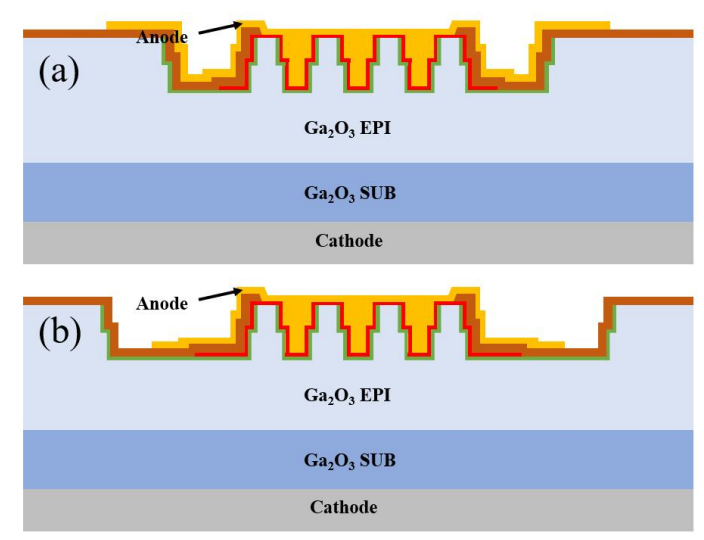
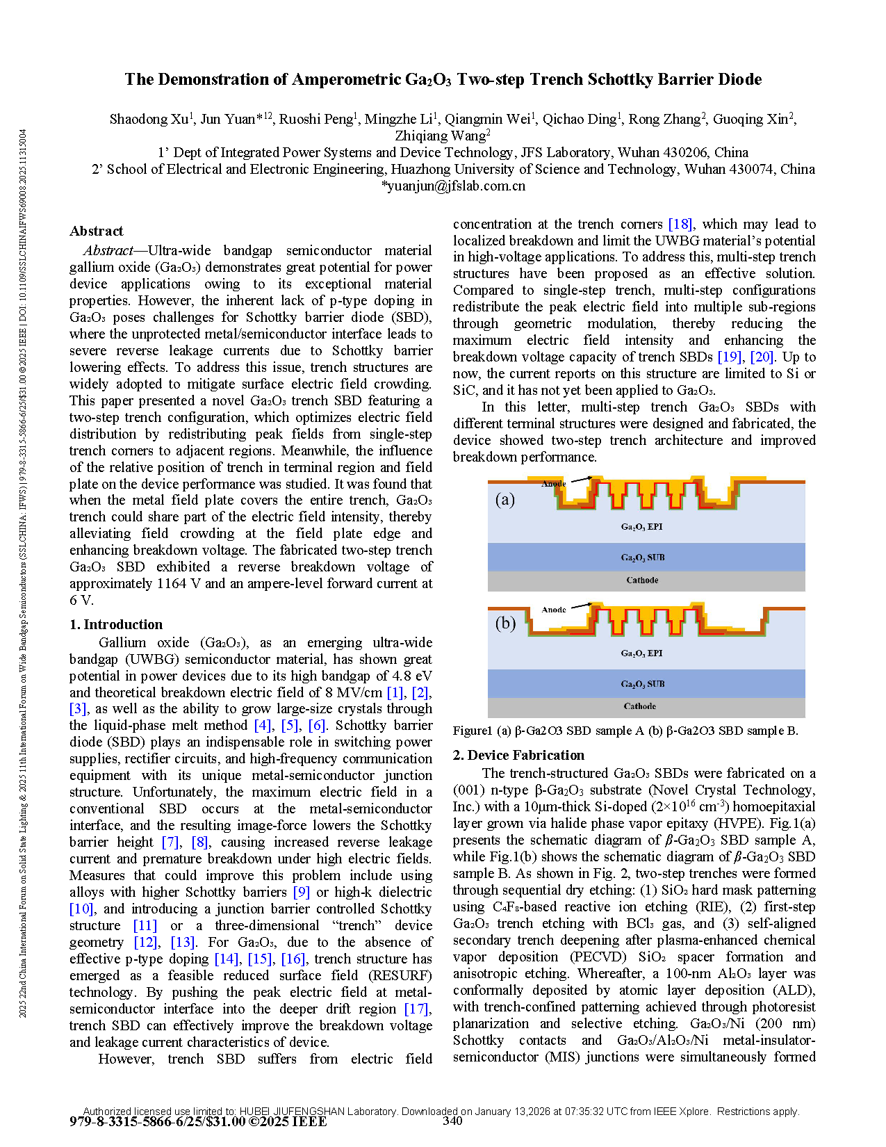
Figure1 (a) β-Ga2O3 SBD sample A (b) β-Ga2O3 SBD sample B.
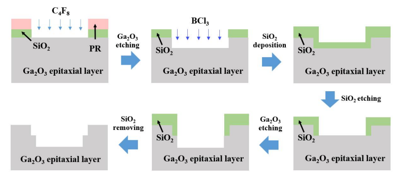
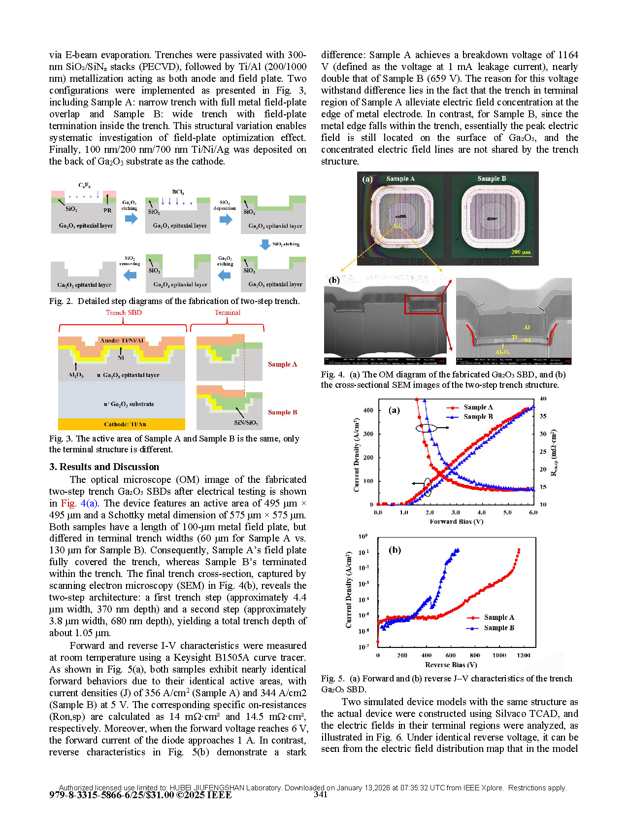
Fig. 2. Detailed step diagrams of the fabrication of two-step trench.
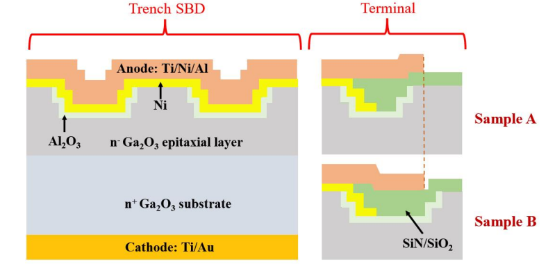
Fig. 3. The active area of Sample A and Sample B is the same, only the terminal structure is different.
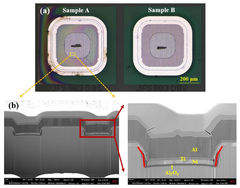
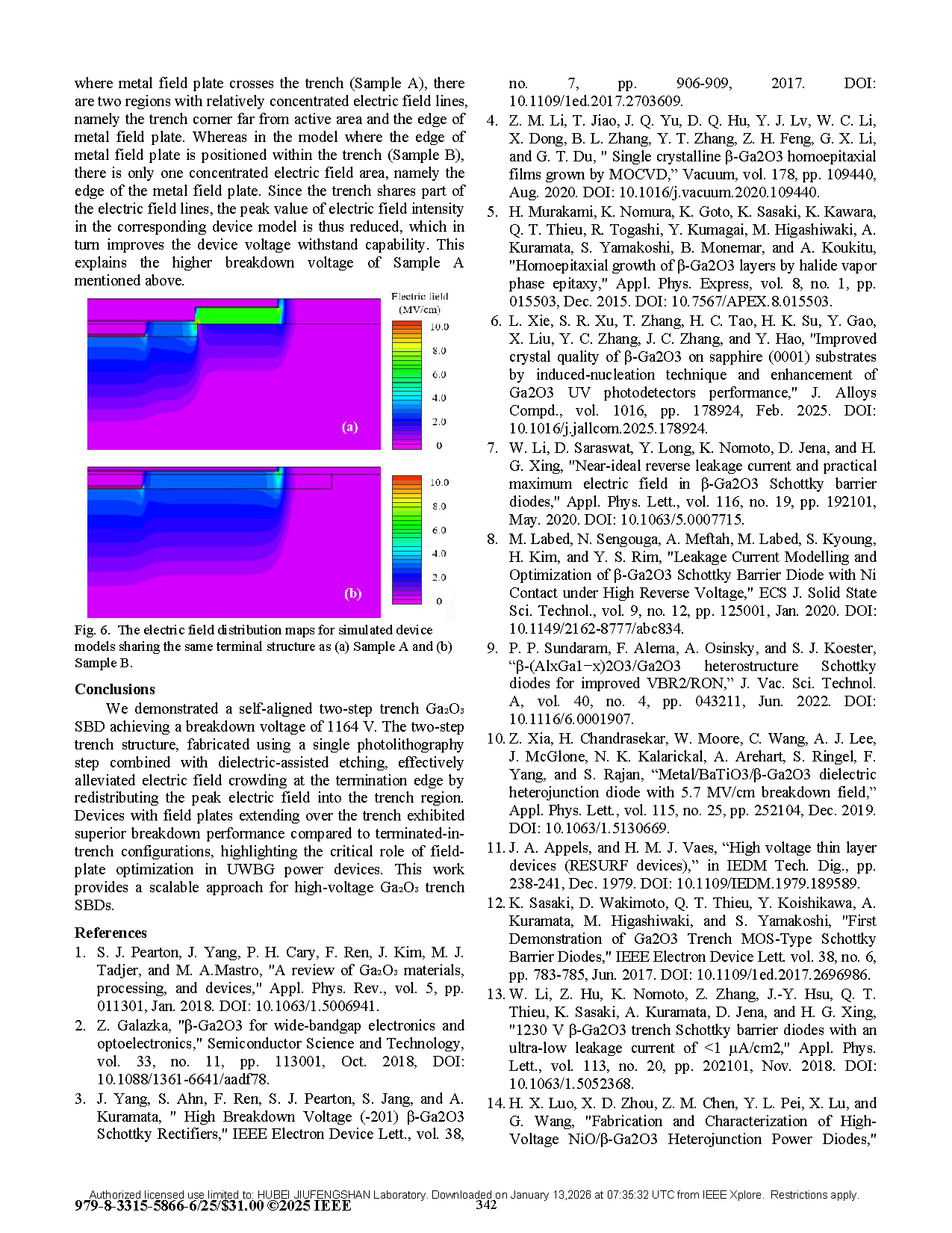
Fig. 4. (a) The OM diagram of the fabricated Ga₂O₃ SBD, and (b) the cross-sectional SEM images of the two-step trench structure.
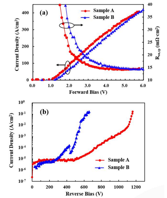
Fig. 5. (a) Forward and (b) reverse J–V characteristics of the trench Ga₂O₃ SBD.
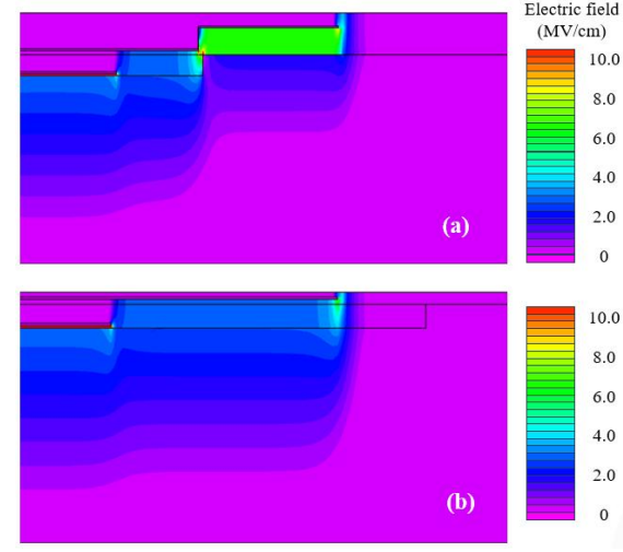
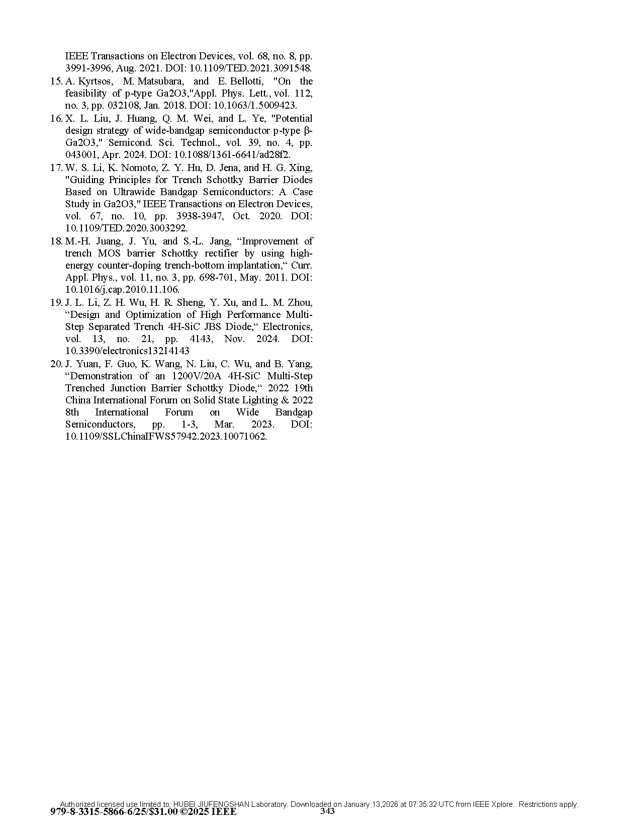
Fig. 6. The electric field distribution maps for simulated device models sharing the same terminal structure as (a) Sample A and (b) Sample B.
DOI:
doi.org/10.1109/SSLCHINAIFWS69008.2025.11315004