Paper Sharing
【Member Papers】Ultrahigh Dielectric Permittivity in Ultrathin 2D β‑Ga₂O₃ for Advanced Dielectric Applications
日期:2026-01-28阅读:530
Researchers from the Suzhou Institute of Nano-Tech and Nano-Bionics,CAS have published a dissertation titled "Ultrahigh Dielectric Permittivity in Ultrathin 2D β-Ga2O3 for Advanced Dielectric Applications" in 2025 22nd China International Forum on Nano Letters.
Abstract
The continuous scaling of semiconductor devices necessitates the integration of high-permittivity (high-k) dielectrics to maintain gate control and reduce power consumption. Here, we report an ultrahigh dielectric constant (k) of ∼150 in ultrathin (10 nm) β-gallium oxide (β-Ga2O3) metal–insulator–metal capacitors. Photoresponse and microstructural analyses link the giant permittivity to an oxygen vacancy (VO)-ordered phase. The fabricated capacitors exhibit excellent performance for memory applications, including low dielectric loss (<0.02 at 100 kHz), low leakage current (<10–7 A/cm2), high operating speed (>20 MHz), and high endurance (>1010 cycles). To validate practical utility, MoS2 field-effect transistors gated by β-Ga2O3 were fabricated, exhibiting a high on/off ratio (>106), a low subthreshold swing (SS) of 68.1 mV/dec, negligible hysteresis (5.8 mV), and ultralow gate leakage (∼10–13 A). These findings establish ultrathin β-Ga2O3 as a compelling high-k material for next-generation logic and memory devices.
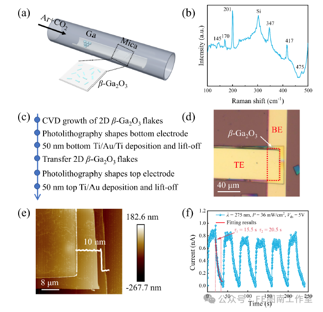
Figure 1. Fabrication, characterization, and electrical performance of β-Ga₂O₃ MIM capacitors.(a) Schematic illustration of the synthesis of β-Ga₂O₃ nanosheets grown on a mica substrate.(b) Raman spectrum of β-Ga₂O₃ nanosheets transferred onto a Si/SiO₂ substrate.(c) Schematic of the key fabrication steps for MIM capacitors using β-Ga₂O₃ as the dielectric layer.(d) Top-view optical microscopy image of a completed capacitor device.(e) AFM image showing the surface morphology.(f) I–t characteristics of β-Ga₂O₃ capacitors measured under dark and illuminated conditions.
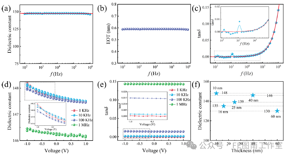 Figure 2. Dielectric properties of β-Ga₂O₃ capacitors.(a,b) Frequency dependence of the dielectric constant (ε′, a) and equivalent oxide thickness (EOT, b) measured under an oscillation field of VOSC = 0.05 V; solid lines represent fits based on Equation (2).(c) Corresponding frequency dependence of the loss tangent (tan δ); the solid line represents a fit based on Equation (3). The inset shows an enlarged view of the low-frequency region.(d,e) Voltage dependence of ε′ and tan δ measured at 1 kHz, 10 kHz, 100 kHz, and 1 MHz, respectively; insets show locally enlarged views.(f) Dielectric constant of MIM capacitors with different thicknesses (10–60 nm) measured at 1 MHz.
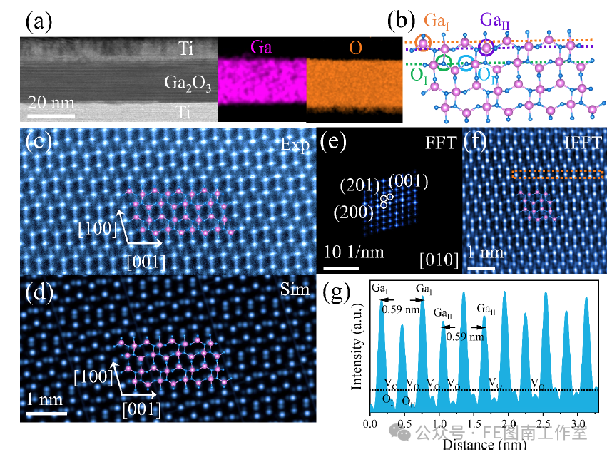 Figure 3. Microstructural and crystallographic characterization of β-Ga₂O₃ capacitors.(a) Low-magnification cross-sectional HAADF-STEM image and corresponding EDS elemental maps of Ga (red) and O (orange).(b) Atomic structure of a two-dimensional β-Ga₂O₃ nanosheet along the [100] crystallographic direction.(c,d) Experimental and simulated HRTEM images of the β-Ga₂O₃ capacitor.(e,f) Fast Fourier transform (FFT) and corresponding inverse FFT images.(g) Intensity line profile along the atomic columns marked by the red dashed box in (f).
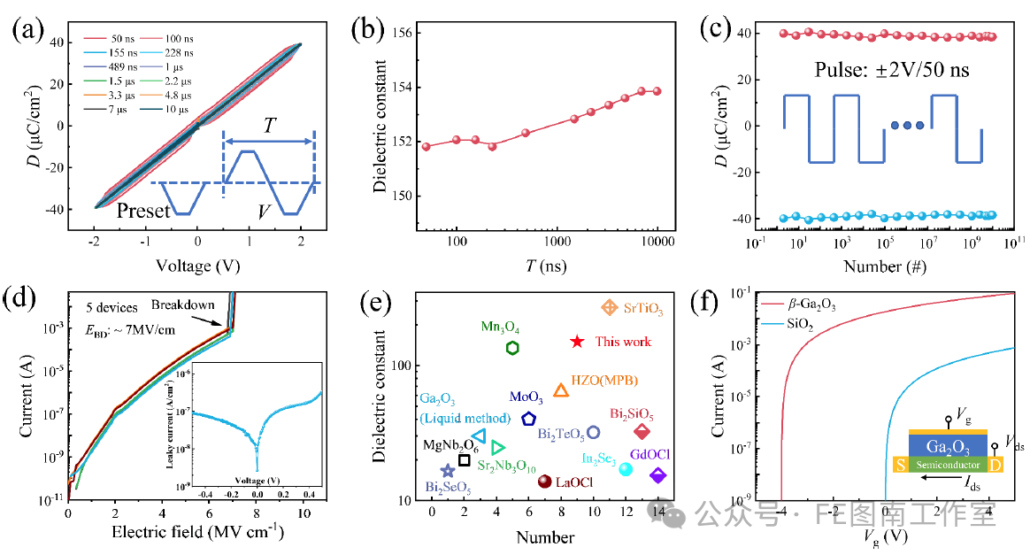 Figure 4. Comprehensive electrical characterization of the high-k performance of β-Ga₂O₃ capacitors.(a) Electric displacement–electric field (D–E) hysteresis loops measured from 20 MHz to 100 kHz; the inset shows the pulse scheme used for D–E measurements.(b) Values of ε′ (in parentheses) estimated from the slopes of the loops in (a).(c) Stored charge density of β-Ga₂O₃ capacitors as a function of cycle number under a unipolar square wave of 2 V / 50 ns at room temperature (repetition frequency: 10 MHz); the inset shows the pulse scheme for endurance testing.(d) Quasi-static I–V characteristics of five independent devices, showing current as a function of applied electric field; arrows indicate breakdown points associated with catastrophic failure. The inset shows leakage current density versus applied voltage (J–V characteristics).(e) Comparison of the dielectric constant achieved in this work with various dielectric materials reported in the literature (Refs. 14, 42, 43, 47–56).(f) Simulated drain current–gate voltage (ID–VG) transfer characteristics of a MOSFET using high-k β-Ga₂O₃ as the top-gate dielectric.
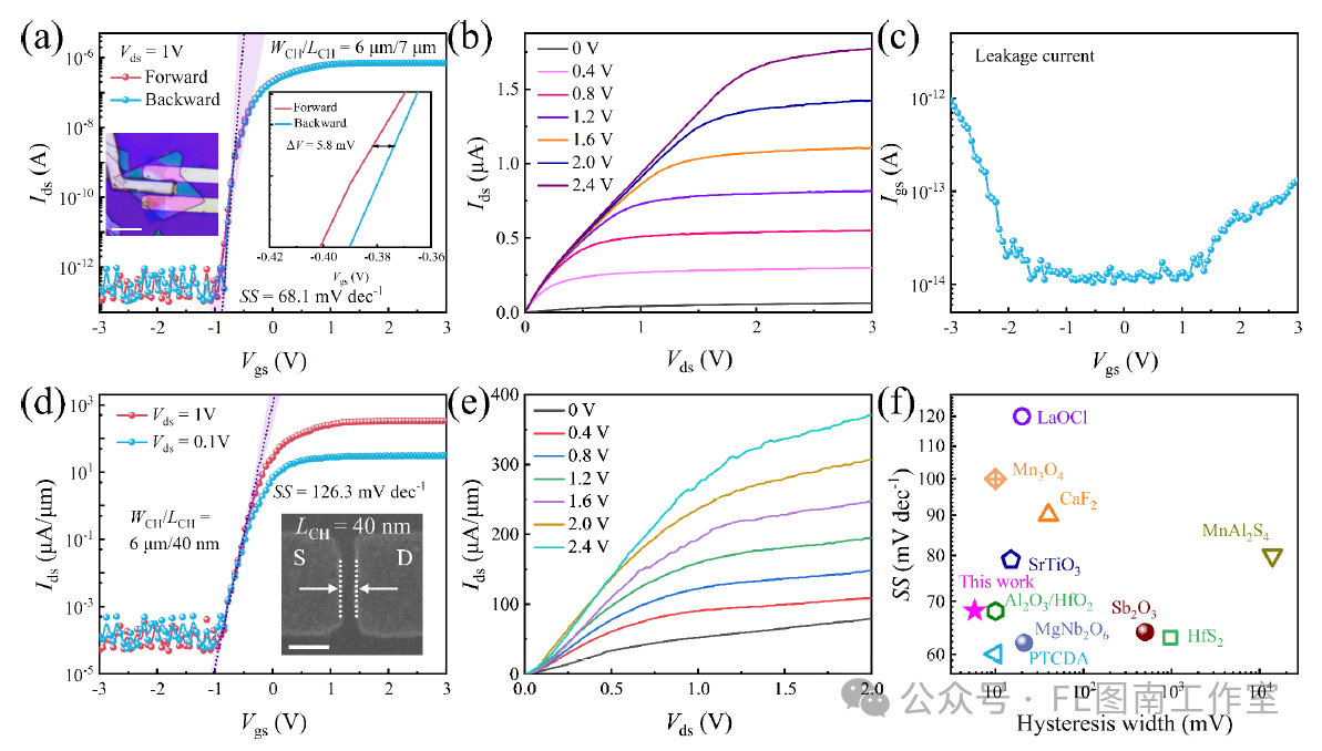 Figure 5. Electrical performance of MoS₂ field-effect transistors employing β-Ga₂O₃ as the top-gate dielectric, fabricated in an oxygen-free glovebox environment.(a) Transfer characteristics (IDS–VGS) measured at VDS = 1 V, showing an on/off ratio > 10⁶, a subthreshold swing of 68.1 mV dec⁻¹, and a hysteresis of 5.8 mV (inset: enlarged view). Inset: optical microscopy image of the device structure. Scale bar: 10 μm. The black solid line denotes the fitting curve, and the purple region represents the 95% confidence interval.(b) Output characteristics (IDS–VDS) measured at stepped VGS values (0–2.4 V), demonstrating current saturation and effective gate modulation.(c) Gate leakage current (IG–VGS) below 10⁻¹³ A, highlighting the excellent insulating quality of the dielectric layer.(d,e) Transfer (d) and output (e) characteristics of a β-Ga₂O₃/MoS₂ FET with a 40 nm channel length. Inset: SEM image of the 40 nm channel in the β-Ga₂O₃/MoS₂ FET. Scale bar: 100 nm.(f) Comparison of subthreshold swing and hysteresis with previously reported dielectric materials (Refs. 48, 51, 54, 55, 57–62), highlighting the superior performance of β-Ga₂O₃.
DOI:
https://doi.org/10.1021/acs.nanolett.5c05733


