Paper Sharing
【Domestic Papers】Thermal tuning of the bandgap in β-(AlₓGa₁₋ₓ)₂O₃/Al₂O₃ heterostructures for tunable photodetector performance
日期:2026-02-03阅读:403
Researchers from the Fuzhou University have published a dissertation titled "Thermal tuning of the bandgap in β-(AlxGa1-x)2O3/Al2O3 heterostructures for tunable photodetector performance" in Optical Materials.
Background
β-gallium oxide (Ga2O3), due to its wide bandgap, low cost, and excellent chemical and thermal stability, has emerged as a key material in the field of fourth-generation semiconductors, driving significant applications such as solar-blind photodetectors high-temperature gas sensors, photoluminescent devices electroluminescent devices, power devices, and resistive switching memory devices. The optical bandgap of β-Ga2O3 is approximately 4.9 eV, corresponding to a wavelength of ∼253 nm in the UV range. However, UV photodetectors are typically employed within the wavelength range of 200–300 nm. Consequently, an effective strategy is urgently required to modulate the bandgap of β-Ga2O3, making it suitable for a broader range of ultraviolet detection wavelengths.
Abstract
The ultrawide-bandgap semiconductor Ga2O3, characterized by its high breakdown voltage, demonstrates significant potential for applications in optoelectronics and photonics. In this study, we propose a cost-effective strategy for the scalable production of Al-doped Ga2O3 via post-growth thermal annealing. Our results demonstrate that the binary β-Ga2O3 films are first alloyed into ternary (-201) β-(AlxGa1-x)2O3 alloys with tunable compositions under optimized annealing conditions, ultimately forming β-(AlxGa1-x)2O3/Al2O3 heterostructures. Specifically, through X-ray diffraction (XRD) analysis, the Al content of the β-Ga2O3 template samples without annealing and annealed up to 1300 °C ranges from 0 to 0.598, with the optical bandgap tunable from 5.01 eV to 6.30 eV. Moreover, the resulting ultraviolet photodetectors based on these composites exhibit enhanced photoresponse performance, with a low dark current of 16.6 fA, a maximum on/off current ratio of 4.53 × 10⁶, and a remarkable responsivity of 5.48 A/W. This study provides a straightforward and efficient approach for tailoring the bandgap of β-(AlxGa1-x)2O3 films for deep-ultraviolet optoelectronic applications.
Highlights
Cost-effective, scalable fabrication of (-201)-oriented β-(AlxGa1−x)2O3/Al2O3 heterostructures.
Al content increases from 0 to 0.598 upon annealing, while the bandgap is tunable from 5.01 to 6.30 eV.
UV photodetectors exhibit a dark current of 16.6 fA, an on/off ratio of 4.53 × 10⁶, and a responsivity of 5.48 A/W.
Conclusions
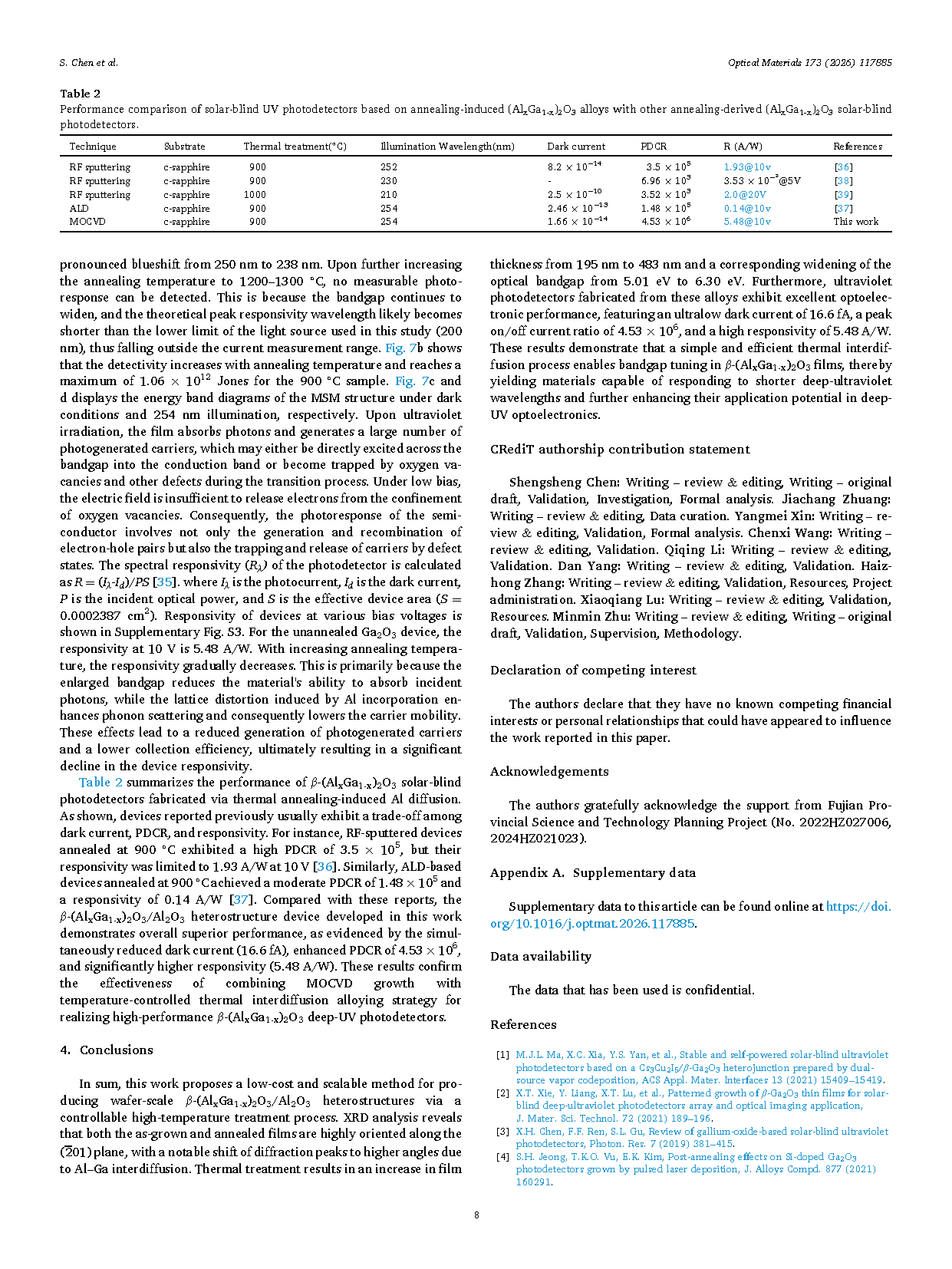
In sum, this work proposes a low-cost and scalable method for producing wafer-scale β-(AlxGa1-x)2O3/Al2O3 heterostructures via a controllable high-temperature treatment process. XRD analysis reveals that both the as-grown and annealed films are highly oriented along the (-201) plane, with a notable shift of diffraction peaks to higher angles due to Al–Ga interdiffusion. Thermal treatment results in an increase in film thickness from 195 nm to 483 nm and a corresponding widening of the optical bandgap from 5.01 eV to 6.30 eV. Furthermore, ultraviolet photodetectors fabricated from these alloys exhibit excellent optoelectronic performance, featuring an ultralow dark current of 16.6 fA, a peak on/off current ratio of 4.53 × 10⁶, and a high responsivity of 5.48 A/W. These results demonstrate that a simple and efficient thermal interdiffusion process enables bandgap tuning in β-(AlxGa1−x)2O3 films, thereby yielding materials capable of responding to shorter deep-ultraviolet wavelengths and further enhancing their application potential in deep-UV optoelectronics.
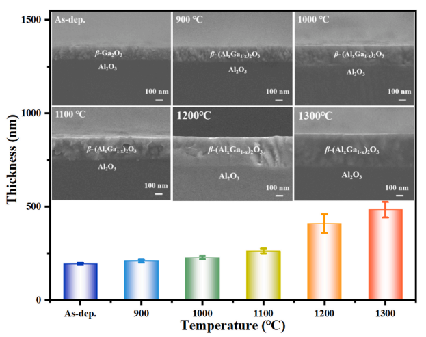
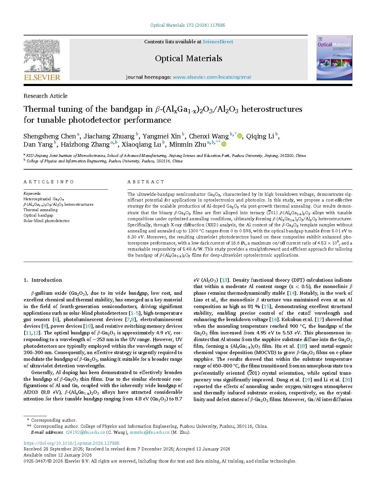
Fig. 1. Evolution of thickness in β-(AlxGa1−x)2O3/Al2O3 heterostructure with annealing temperature. The insets show the SEM images of the corresponding sample.
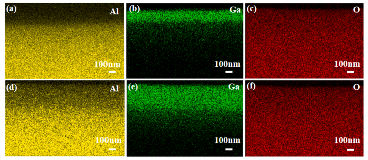
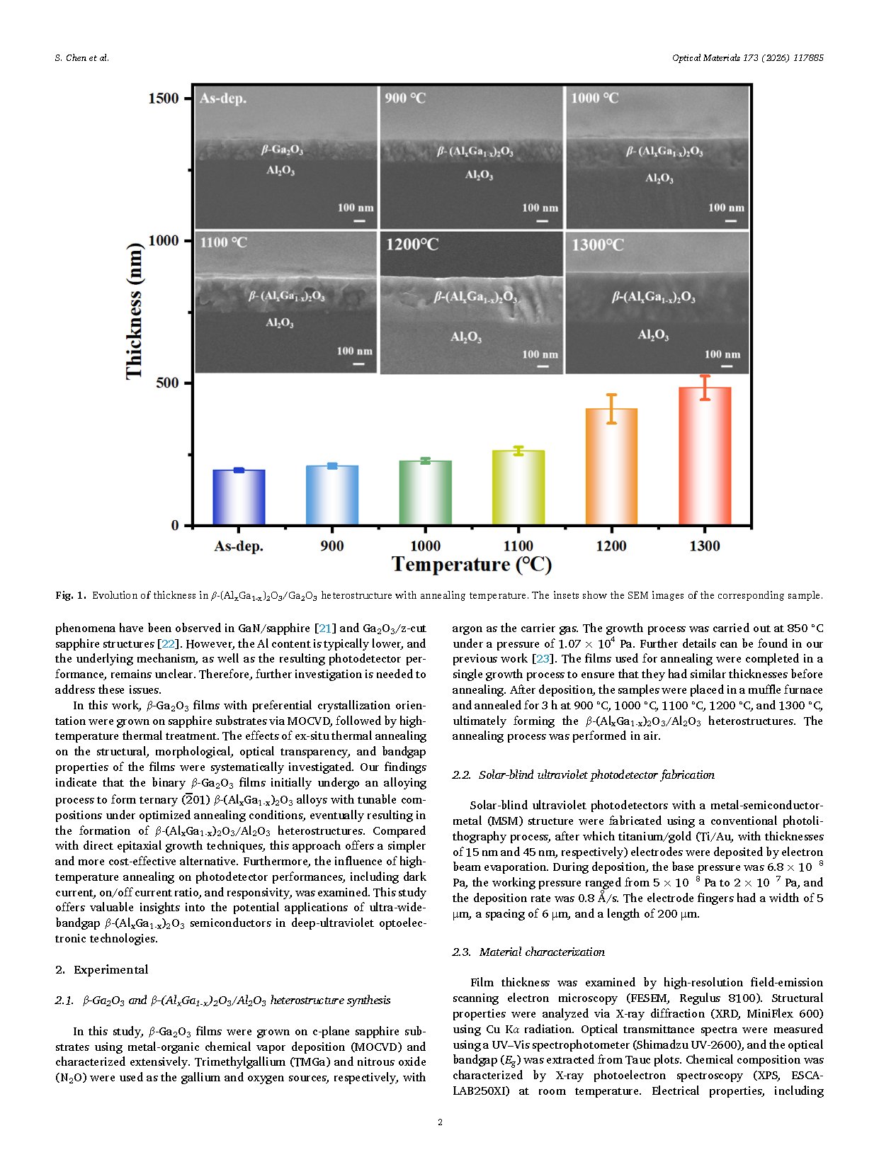
Fig. 2. EDS analysis of films at an annealing temperature of 1000 °C: (a) Al, (b) Ga and (c) O; EDS analysis of films at an annealing temperature of 1300 ◦C: (d) Al, (e) Ga and (f) O.
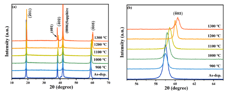
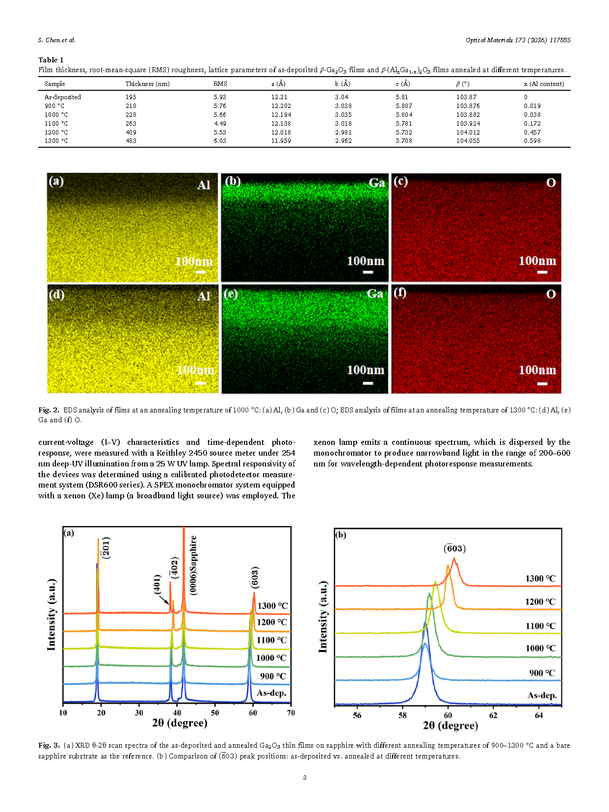
Fig. 3. (a) XRD θ-2θ scan spectra of the as-deposited and annealed Ga2O3 thin films on sapphire with different annealing temperatures of 900–1300 °C and a bare sapphire substrate as the reference. (b) Comparison of (-603) peak positions: as-deposited vs. annealed at different temperatures.

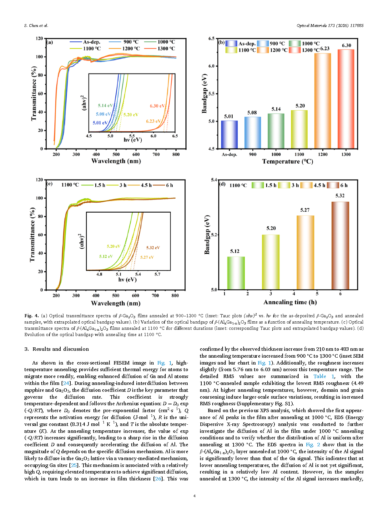
Fig. 4. (a) Optical transmittance spectra of β-Ga2O3 films annealed at 900–1300 °C (inset: Tauc plots (αhν)2 vs. hν for the as-deposited β-Ga2O3 and annealed samples, with extrapolated optical bandgap values). (b) Variation of the optical bandgap of β-(AlxGa1−x)2O3 films as a function of annealing temperature. (c) Optical transmittance spectra of β-(AlxGa1−x)2O3 films annealed at 1100 ◦C for different durations (inset: corresponding Tauc plots and extrapolated bandgap values). (d) Evolution of the optical bandgap with annealing time at 1100 °C.
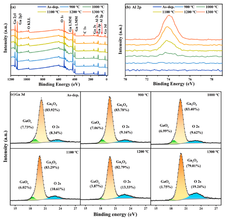
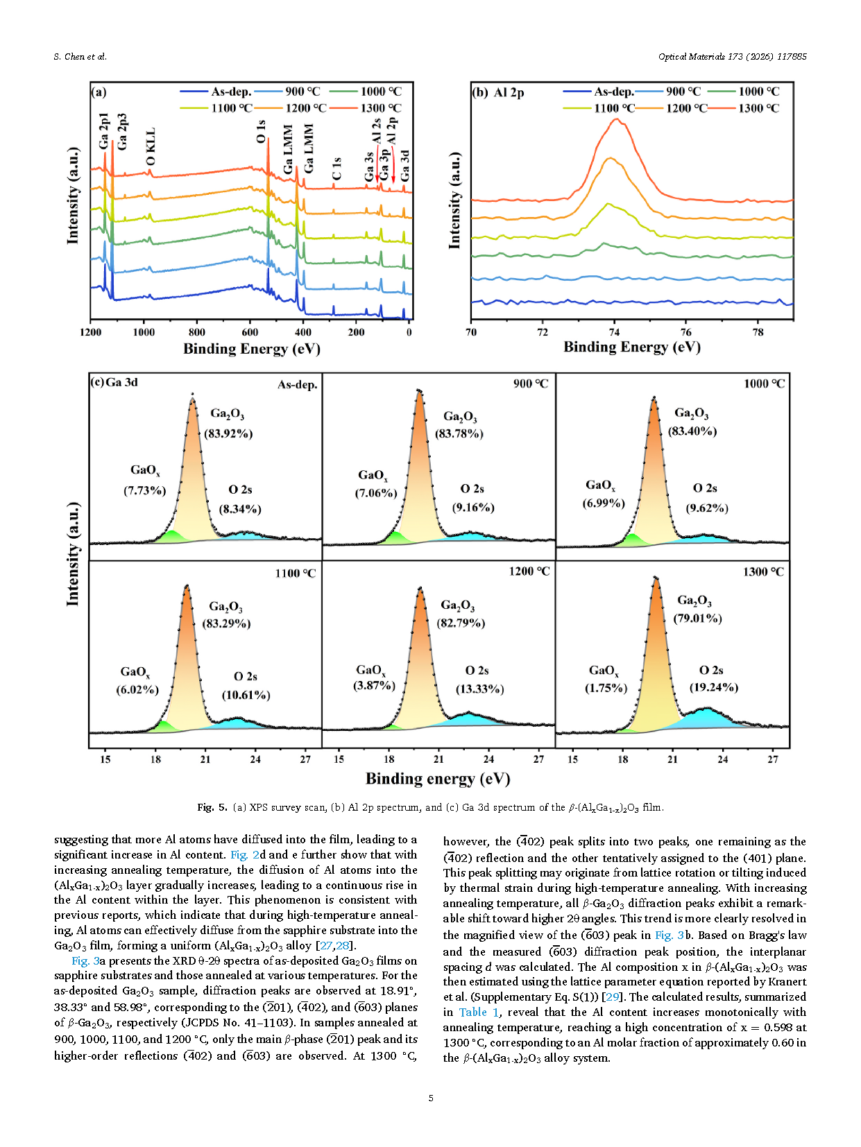
Fig. 5. (a) XPS survey scan, (b) Al 2p spectrum, and (c) Ga 3d spectrum of the β-(AlxGa1−x)2O3 film.
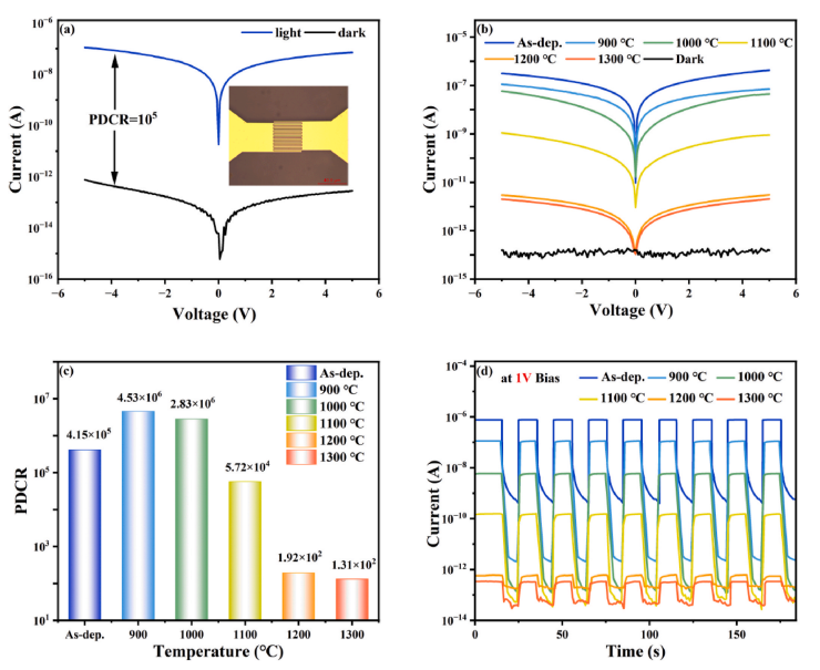
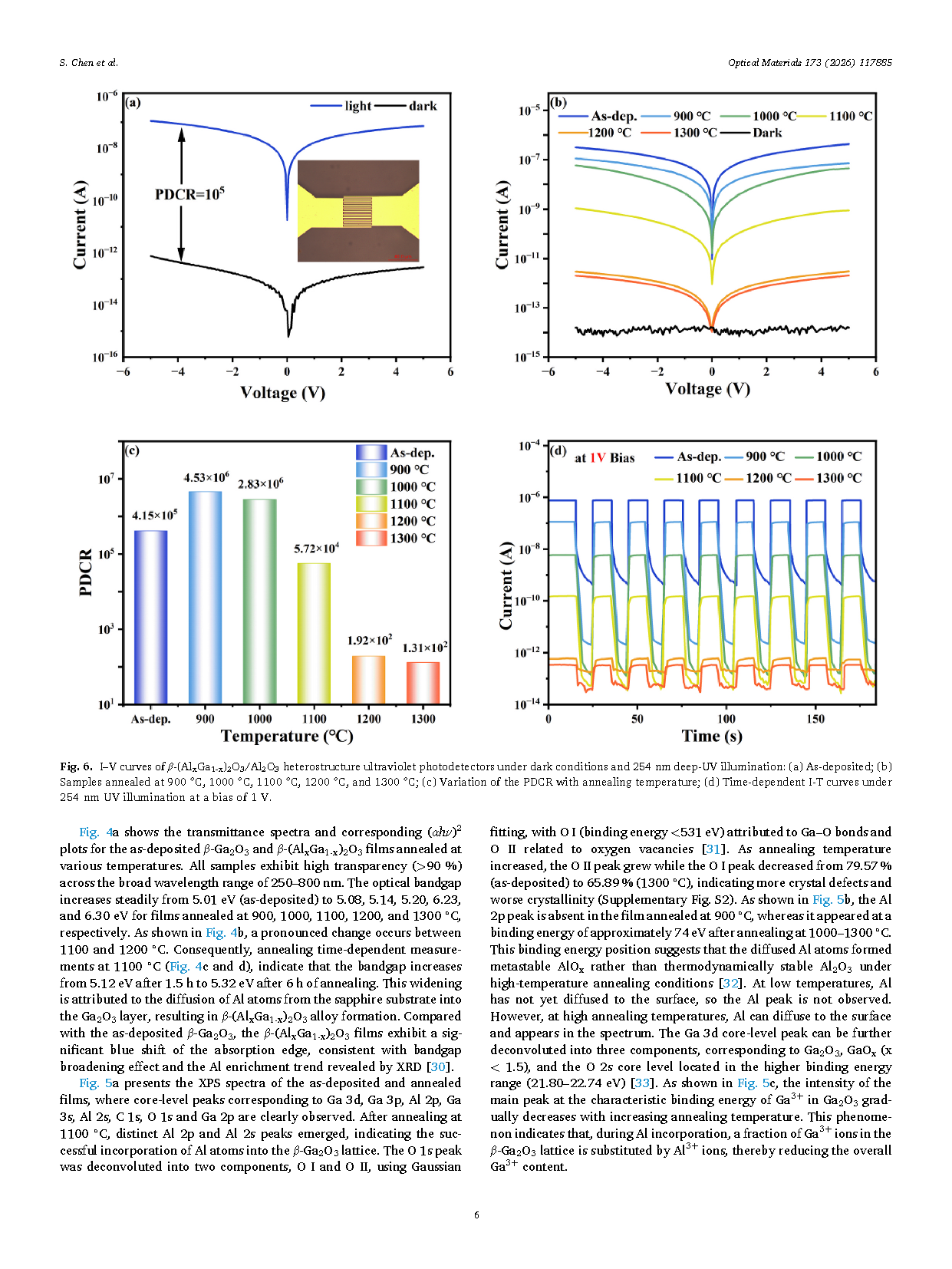
Fig. 6. I–V curves of β-(AlxGa1−x)2O3/Al2O3 heterostructure ultraviolet photodetectors under dark conditions and 254 nm deep-UV illumination: (a) As-deposited; (b) Samples annealed at 900 °C, 1000 °C, 1100 °C, 1200 °C, and 1300 °C; (c) Variation of the PDCR with annealing temperature; (d) Time-dependent I-T curves under 254 nm UV illumination at a bias of 1 V.
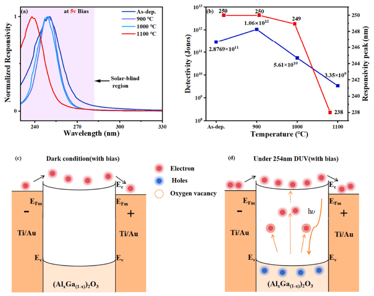
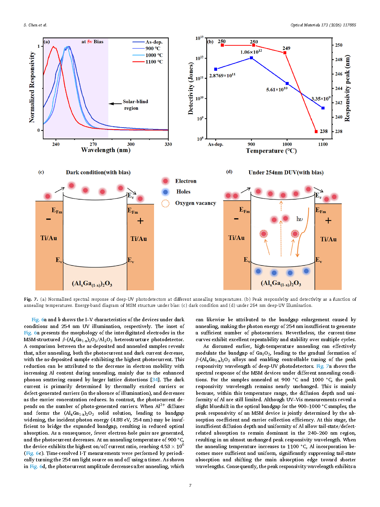
Fig. 7. (a) Normalized spectral response of deep-UV photodetectors at different annealing temperatures. (b) Peak responsivity and detectivity as a function of annealing temperatures. Energy-band diagram of MSM structure under bias: (c) dark condition and (d) under 254 nm deep-UV illumination.
DOI:
doi.org/10.1016/j.optmat.2026.117885