Paper Sharing
【Member Papers】Epitaxial Growth of Degenerately Doped Ga₂O₃ Films on GaN (0001) as a Deep Ultraviolet Transparent Electrode for Opto-Electronics Applications
日期:2026-02-04阅读:418
Researchers from the Xiamen University have published a dissertation titled "Epitaxial Growth of Degenerately Doped Ga2O3 Films on GaN (0001) as a Deep Ultraviolet Transparent Electrode for Opto-Electronics Applications" in Advanced Optical Materials.
Project Support
This work was supported by the Shenzhen Science and Technology Innovation Committee (Grant No. JCYJ20240813145501003), the National Natural Science Foundation of China (Grant No. 22275154), and the Science & Technology Commission of Shanghai Municipality (Grant No. 25JD1404600).
Background
Deep ultraviolet (DUV, 200–300 nm) transparent conducting oxides (TCOs) have garnered significant research interest as transparent electrodes for DUV optoelectronic devices, such as laser diodes (LDs), light-emitting diodes (LEDs), and solar-blind photodetectors (SBPDs). DUV LEDs play a crucial role in various applications such as sterilization, water purification, lithography, biological detection, and optical communication systems. The development of GaN-based DUV LEDs in recent years has further advanced the LED industry into the DUV spectral region. However, the external quantum efficiency (EQE) of these devices is quite low (only ≈1%), in part because of the non-availability of a deep UV transparent electrode. Conventional TCO materials such as Sn-doped In2O3 (ITO), F-doped SnO2 (FTO), and Al-doped ZnO (AZO) are opaque in the deep UV region because of their small Eg of less than 3.5 eV. Hence, the development of new TCOs with high DUV transparency and conductivity is imperative for advancing DUV optoelectronics devices.
Abstract
GaN-based deep ultraviolet (DUV) optoelectronic devices have garnered considerable attention for applications in sterilization, biological detection, and optical communications. However, the performance of current DUV optoelectronic devices is limited by the insufficient DUV transparency of conventional electrodes. In this work, the epitaxial growth of degenerately Si-doped Ga2O3 films on GaN as a promising DUV transparent electrode is reported. The 0.5% Si doped Ga2O3 (n+-Ga2O3) films exhibit DUV transparency exceeding 85% in the spectral range from 280 to 400 nm wavelength. Such a high DUV transparency is attributed to the ultrawide bandgap of ≈5.0 eV of the n+-Ga2O3 film induced by the Burstein–Moss effect due to degenerate doping. Moreover, the n+-Ga2O3 film exhibits a very low specific contact resistance of 1.96 × 10⁻⁴ Ω cm2 to GaN. High-resolution X-ray photoemission spectroscopic (XPS) study reveals that n+-Ga2O3 forms a type-II staggered band alignment with GaN with a low interface barrier of 0.15 eV and a narrow band bending thickness of a few nm. The small barrier, together with the degenerately doped Ga2O3 film, enables excellent electrical contact at the n+-Ga2O3/GaN interface and low contact resistance. This work demonstrates n+-Ga2O3 as a promising alternative for DUV transparent electrode for GaN-based DUV devices.
Conclusion
In this work, we report the epitaxial growth of n+-Ga2O3 thin films on (0001)-oriented GaN as a new DUV transparent electrode. Our n+-Ga2O3 films exhibit exceptional optical performance, with > 85% transparency in the 280–400 nm wavelength range, attributed to the ultra-wide bandgap (≈5.0 eV) of n+-Ga2O3, which is further widened by the Burstein-Moss effect. Moreover, these films achieve a low specific contact resistance of 1.96 × 10⁻⁴ Ω cm2 to GaN. Detailed high-resolution XPS quantitative analysis at the interface reveals that the low specific contact resistance at the n+-Ga2O3/GaN interface can be attributed to the favorable interfacial energetics with a low interface barrier of 0.15 eV and a narrow band bending thickness of a few nm. The low barrier and the narrow band bending enable efficient carrier transport via tunneling, facilitating the establishment of good Ohmic contact. The excellent ohmic contact and high DUV transmittance demonstrate n+-Ga2O3 as a promising alternative for DUV transparent electrode for GaN-based DUV devices. However, the resistivity of the n+-Ga2O3 thin films in this work (≈0.17 Ω cm) is still higher than that of traditional TCO materials (10−4–10−3 Ω cm). To meet the electrode requirements for practical applications, it has to sacrifice optical transparency and appropriately increase the electrode thickness. Such a trade-off strategy based on performance compromise is hard to fully exploit the application potential of this DUV transparent electrode. Future work will focus on improving its carrier mobility and doping efficiency to further optimize the comprehensive performance.
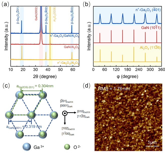
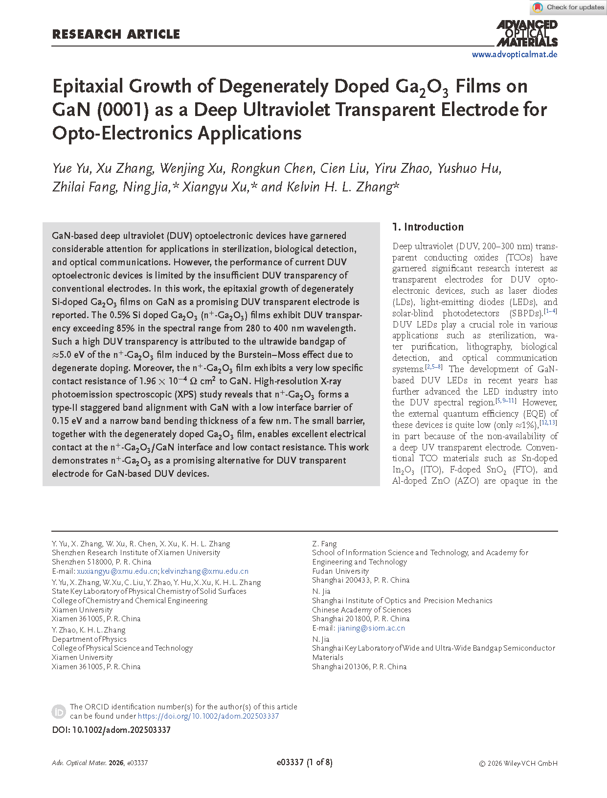
Figure 1. a) XRD patterns of GaN, n+-Ga2O3, and n+-Ga2O3 /GaN heterojunction samples on Al2O3 (0001) substrates. b) φ-scans from (-401), (10-11), and (11-26) planes of n+-Ga2O3, GaN thin film and Al2O3 substrate, respectively. c) Schematic diagrams of epitaxial relationships of n+-Ga2O3 (-201) and GaN (0001) from the top view. d) AFM image of the n+-Ga2O3 film.
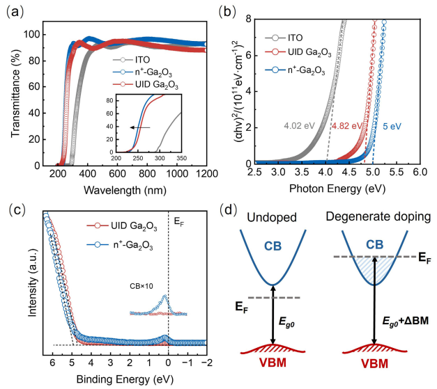
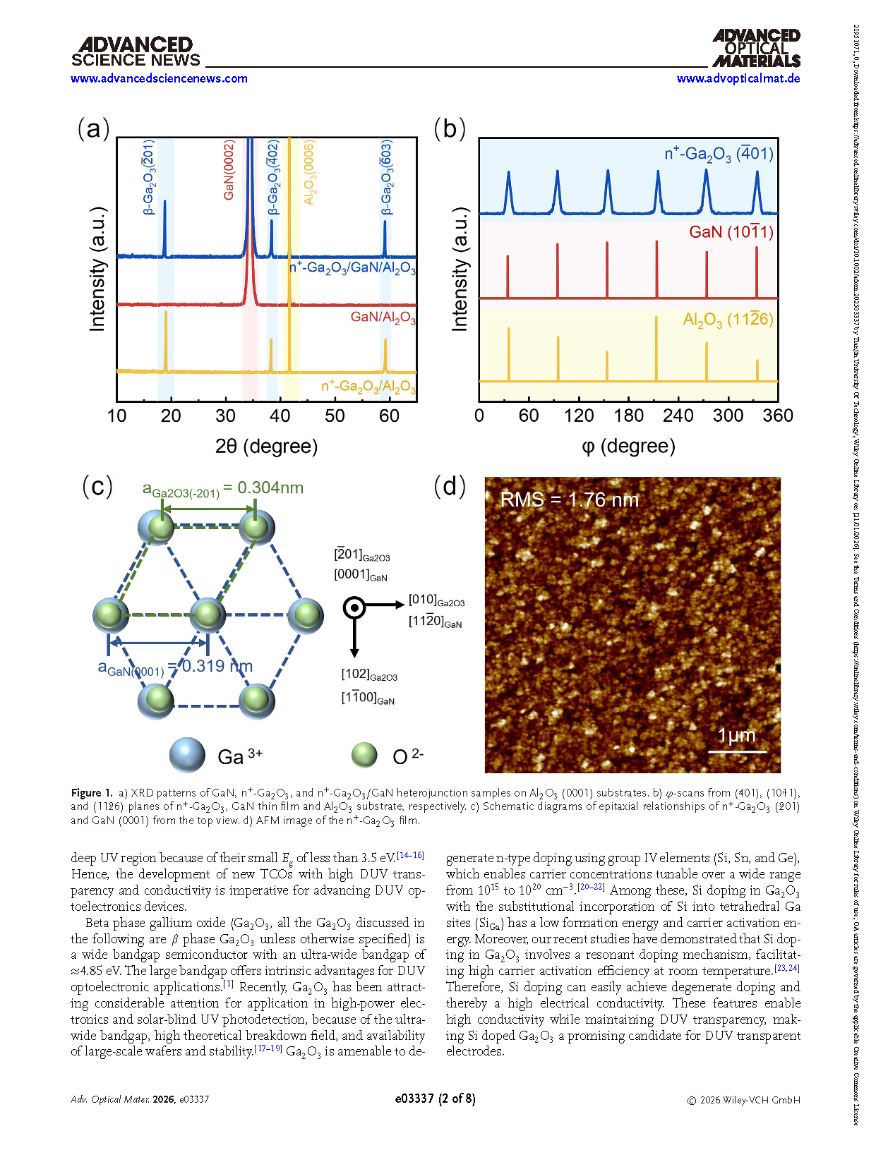
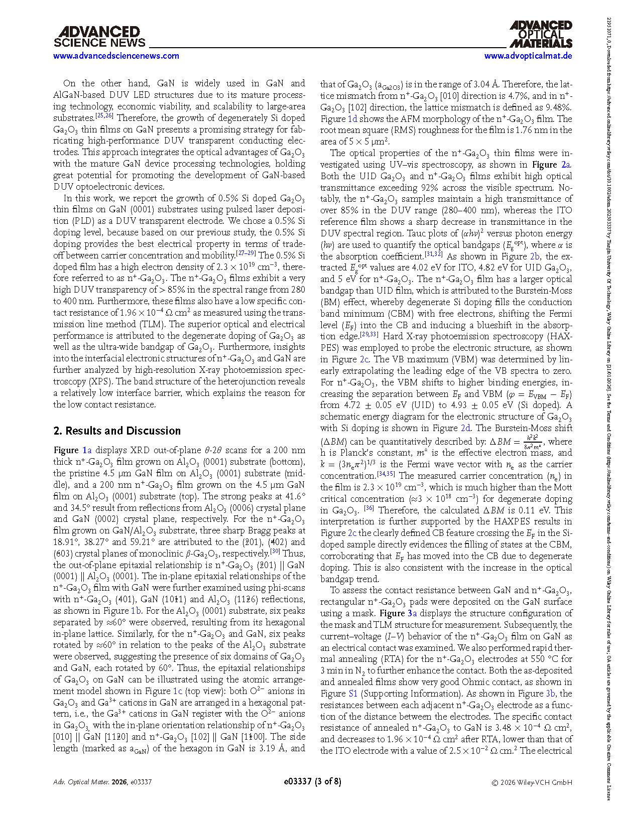
Figure 2. a) Optical transmission of n+-Ga2O3, UID Ga2O3, and ITO on Al2O3(0001) substrates(inset: enlarged absorption edges). b) Plots of (αhv)2 versus hv for the extrapolation of bandgaps of n+-Ga2O3, UID Ga2O3, and ITO on Al2O3 (0001) substrates. c) VBMs of n+-Ga2O3 and UID Ga2O3 with 10 times CBs. d) Schematic electronic structures of undoped Ga2O3 and the change of bandgaps after degenerate doping resulting from the free-electron model.
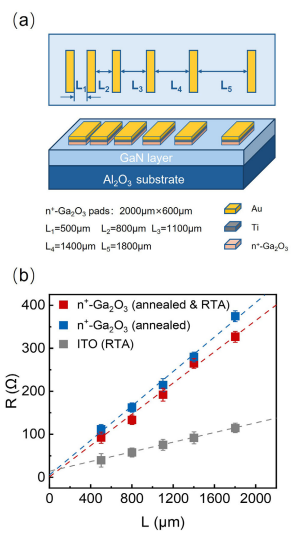
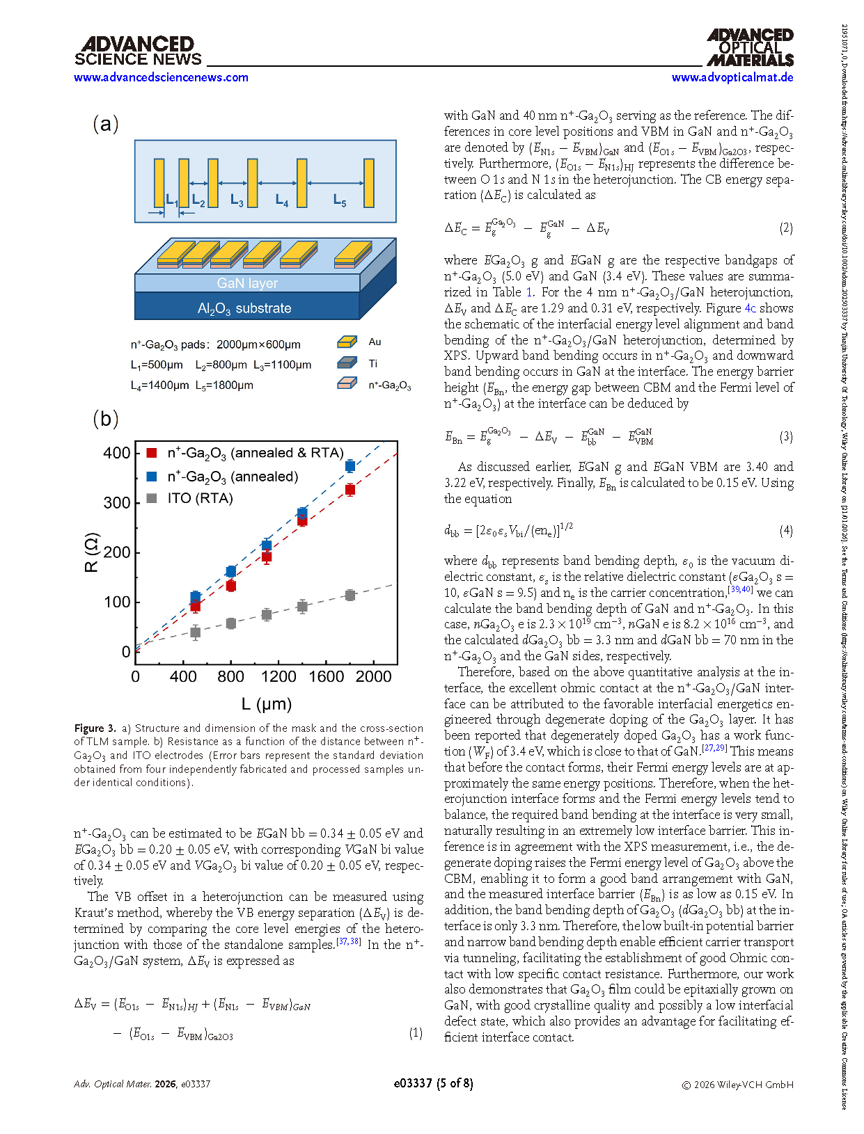
Figure 3. a) Structure and dimension of the mask and the cross-section of TLM sample. b) Resistance as a function of the distance between n+-Ga2O3 and ITO electrodes (Error bars represent the standard deviation obtained from four independently fabricated and processed samples under identical conditions).
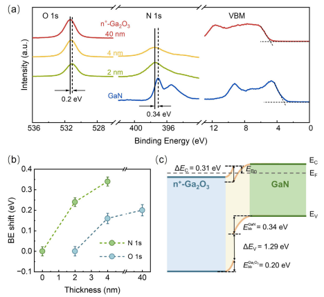
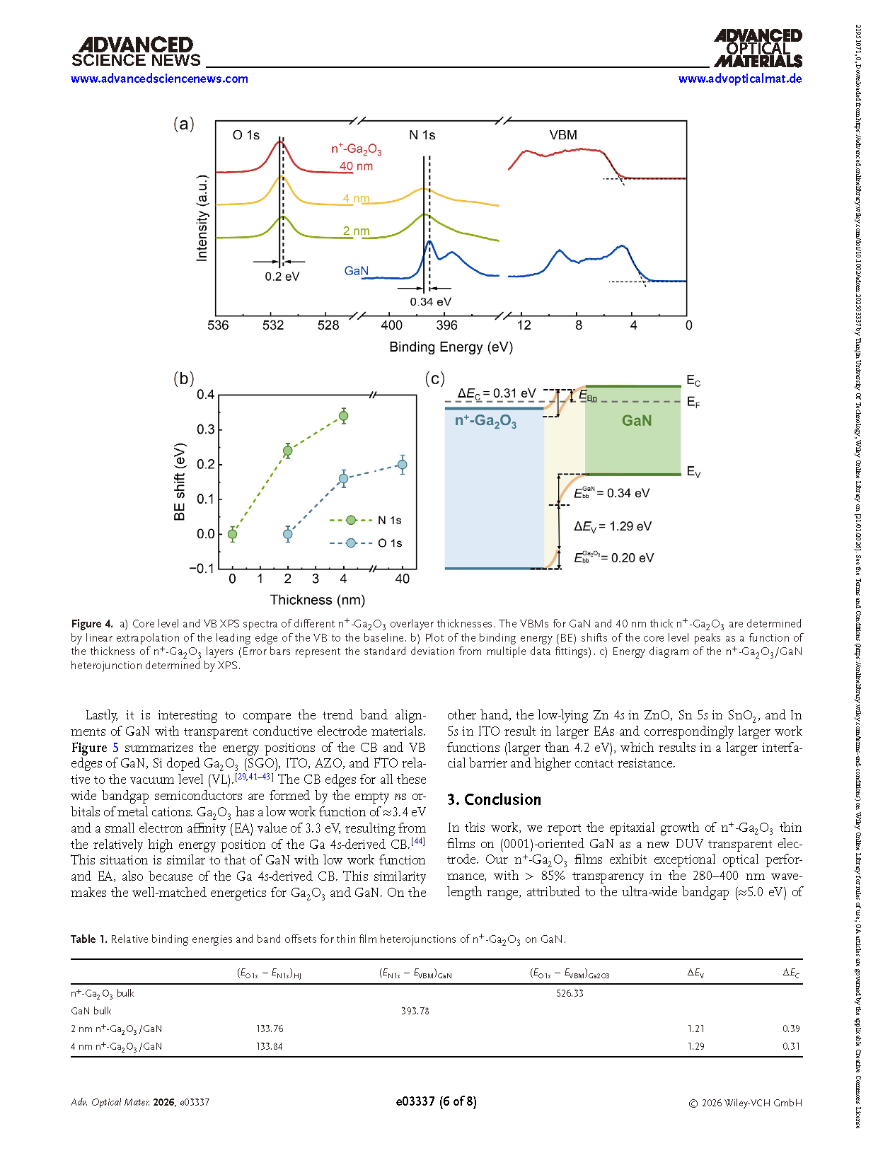
Figure 4. a) Core level and VB XPS spectra of different n+-Ga2O3 overlayer thicknesses. The VBMs for GaN and 40 nm thick n+-Ga2O3 are determined by linear extrapolation of the leading edge of the VB to the baseline. b) Plot of the binding energy (BE) shifts of the core level peaks as a function of the thickness of n+-Ga2O3 layers (Error bars represent the standard deviation from multiple data fittings). c) Energy diagram of the n+-Ga2O3/GaN heterojunction determined by XPS.
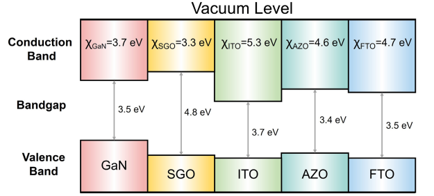
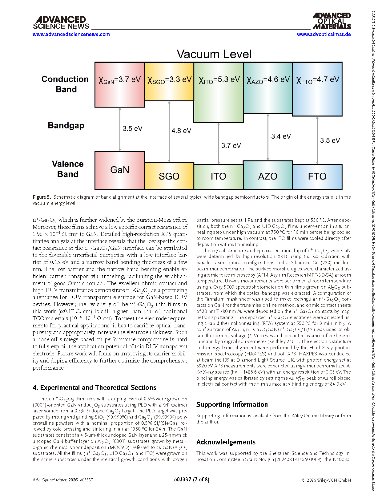
Figure 5. Schematic diagram of band alignment at the interface of several typical wide bandgap semiconductors. The origin of the energy scale is in the vacuum energy level.
DOI:
doi.org/10.1002/adom.202503337