Member Intro
【Member Intro】School of Materials Science and Engineering, Harbin Institute of Technology—— Regular Member
日期:2026-02-25阅读:661
1、 Unit Introduction
The School of Materials Science and Engineering was established in 1952 and is among the first national doctoral degree authorization points, first national postdoctoral mobile stations, and one of the earliest key disciplines selected for China’s “Double First-Class” initiative. The school’s first-round Double First-Class evaluation was rated as “significantly effective,” and it has been promoted to the “Excellence Discipline” category. The school currently hosts eight national-level platforms, including the National Key Laboratory of Precision Welding and Joining of Materials, National Key Laboratory of Space Environment and Material Interaction, National Key Laboratory of Precision Thermal Processing of Metals, and the National Teaching and Experimental Demonstration Center for Materials Science and Engineering, providing students with world-class platforms to cultivate innovation and practical skills. The faculty includes four academicians of the Chinese Academy of Engineering and 51 national-level high-end talents. The school emphasizes a talent cultivation philosophy of “solid foundation, strong practice, rigorous process, and pursuit of innovation,” and is the first in China to implement a fully integrated “Bachelor–Master–Doctor” training pathway, annually admitting over 300 undergraduates, 300 master’s students, and 200 doctoral students.

2、 R&D Team
The Extreme Environment Materials and Device Technology Innovation Center integrates expertise across eight disciplines, including materials science, integrated circuits, physics, and computer science. The center has assembled a multidisciplinary team composed of 10 full professors, 5 associate professors, 5 postdoctoral researchers, and over 30 engineers. Addressing the urgent demand for high-reliability and long-lifespan materials and devices in extreme service environments, the team focuses on process modeling, physical modeling, and multi-physics coupling algorithms for semiconductor functional materials/devices, as well as functional material/device design, reliability evaluation theory, and ground test verification methods. The center’s self-developed software platform has overcome technical bottlenecks in large-scale electronic structure computation and dynamic material evolution under extreme multi-physics fields, enabling automated and parallelized high-efficiency simulations that couple realistic process conditions, application scenarios, and physical processes. In recent years, the team has achieved significant results in co-optimization of electronic device materials, processes, and performance, as well as radiation-hardening processes for electronic devices, with research published in international journals such as Nature Electronics and IEEE Transactions on Nuclear Science, and has undertaken multiple major national research projects. Based on these research directions, the team recruits over 20 doctoral students and more than 50 master’s students annually.

Selected Achievements of the Extreme Environment Materials and Device Technology Innovation Center
3、 Achievement Presentation
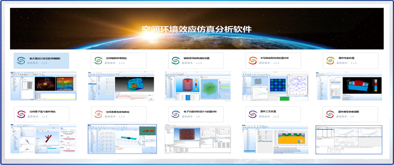
Space Environment Effect Simulation and Analysis Software Platform (ERETCAD)
The ERETCAD platform integrates 11 self-developed software packages, including four CAE tools for spacecraft operational status and environment simulation, atomic oxygen and UV effects, surface charging and discharging effects, and space radiation environment effects; and seven EDA tools for material design and simulation, radiation-induced defect evolution, semiconductor defect property simulation, device process simulation, device performance simulation, device model parameter extraction, and device radiation effect simulation. The platform enables real-time dynamic multi-scale simulation across spacecraft, materials, and devices, integrating first-principles, molecular dynamics, Monte Carlo, and kinetic Monte Carlo methods. It supports large-scale electronic structure computation, defect evolution kinetics under radiation, precise defect property simulation, and device performance degradation simulation, providing a full-chain simulation from environment → material → process → device → spacecraft.

Multi-Level Integrated Simulation of Space Environment Effects
Space Environment Effect Simulation and Analysis Software Platform (ERETCAD)
Radiation Damage Assessment of Gallium Oxide Materials and Devices
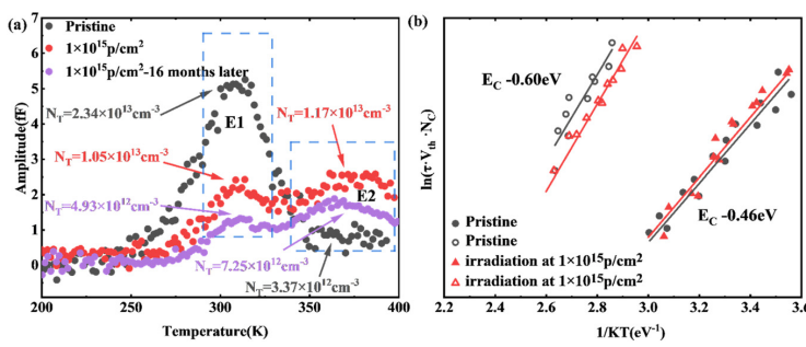
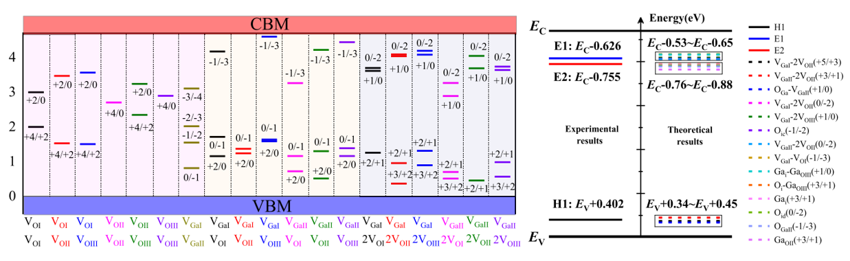
The center has conducted γ-ray, electron, proton, and heavy-ion radiation damage assessments for Gallium Oxide materials and devices. Results show that Gallium Oxide devices exhibit good γ-ray radiation tolerance; electron irradiation introduces deep-level defects (e.g., E2, E1, H1), causing significant electrical performance degradation, some of which can be repaired by annealing. Proton irradiation at 170 keV improves Gallium Oxide SBD device performance by reducing turn-on voltage, increasing current density, and lowering leakage current, with defect evolution dominated by hydrogen passivation as the key physical mechanism. Proton irradiation at 3–10 MeV gradually reduces displacement damage, while heavy-ion irradiation increases vacancy defects (especially VO and VGa–VO), leading to lattice distortion and reduced photoluminescence. Most defects exhibit non-radiative recombination, suppressing light emission. The ERETCAD software guides radiation damage experiments on Gallium Oxide SBD devices.
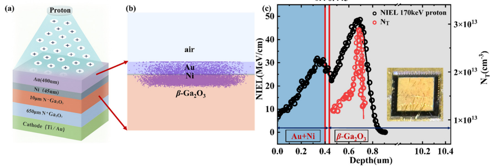
ERETCAD Software Guides Radiation Damage Experiments on Gallium Oxide SBD Devices
Quantitative Characterization and Precise Identification of Radiation-Induced Defects
Using Deep-Level Transient Spectroscopy (DLTS), the team quantitatively characterizes radiation-induced defects in Gallium Oxide devices, including defect energy levels, concentrations, and capture cross-sections. By combining this with a Gallium Oxide defect database constructed via ERET CAD (covering approximately 200 defect types), the team achieves precise definition of defect structures and types, revealing the underlying physical mechanisms of damage from different particle irradiation, which is critical for enhancing Gallium Oxide device radiation tolerance.
DLTS Defect Characterization
Defect Database and Defect Identification
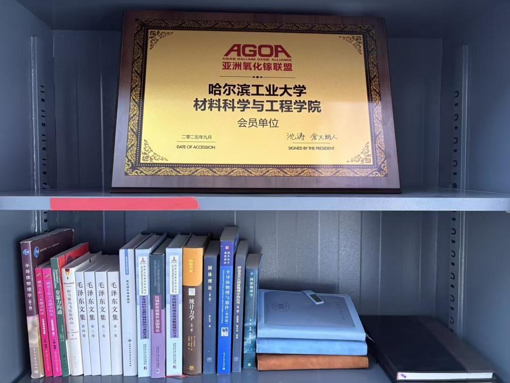
4、Member Bronze Plaque Presentation and Photo Session